 https://silvaco.com/wp-content/uploads/2020/03/simstd_Q1_2015_hints3.jpg
1012
782
Ingrid Schwarz
/wp-content/uploads/2019/11/silvaco-logo.png
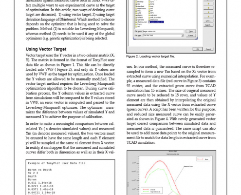
Ingrid Schwarz2015-01-01 10:38:492021-10-13 10:01:42Hints, Tips, and Solutions – Defining VWF Curve Target For Curve Calibration
https://silvaco.com/wp-content/uploads/2020/03/simstd_Q1_2015_hints3.jpg
1012
782
Ingrid Schwarz
/wp-content/uploads/2019/11/silvaco-logo.png
Ingrid Schwarz2015-01-01 10:38:492021-10-13 10:01:42Hints, Tips, and Solutions – Defining VWF Curve Target For Curve Calibration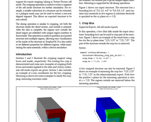 https://silvaco.com/wp-content/uploads/2020/03/simstd_Q1_2015_hints2.jpg
1012
782
Ingrid Schwarz
/wp-content/uploads/2019/11/silvaco-logo.png
Ingrid Schwarz2015-01-01 10:35:272021-10-13 10:01:42Hints, Tips, and Solutions – Crop and Slice in the Victory Process 3D Exports
https://silvaco.com/wp-content/uploads/2020/03/simstd_Q1_2015_hints2.jpg
1012
782
Ingrid Schwarz
/wp-content/uploads/2019/11/silvaco-logo.png
Ingrid Schwarz2015-01-01 10:35:272021-10-13 10:01:42Hints, Tips, and Solutions – Crop and Slice in the Victory Process 3D Exports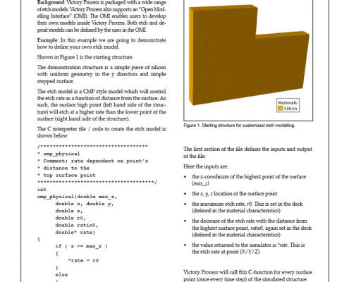 https://silvaco.com/wp-content/uploads/2020/03/simstd_Q1_2015_hints1.jpg
1012
782
Ingrid Schwarz
/wp-content/uploads/2019/11/silvaco-logo.png
Ingrid Schwarz2015-01-01 10:29:242021-10-13 10:01:42Hints, Tips and Solutions – Develop your own etch model in Victory Process
https://silvaco.com/wp-content/uploads/2020/03/simstd_Q1_2015_hints1.jpg
1012
782
Ingrid Schwarz
/wp-content/uploads/2019/11/silvaco-logo.png
Ingrid Schwarz2015-01-01 10:29:242021-10-13 10:01:42Hints, Tips and Solutions – Develop your own etch model in Victory Process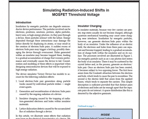 https://silvaco.com/wp-content/uploads/2020/03/simstd_Q4_2014_a1.jpg
1012
782
Ingrid Schwarz
/wp-content/uploads/2019/11/silvaco-logo.png
Ingrid Schwarz2014-10-01 23:10:272021-10-13 10:20:55Simulating Radiation-Induced Shifts in MOSFET Threshold Voltage
https://silvaco.com/wp-content/uploads/2020/03/simstd_Q4_2014_a1.jpg
1012
782
Ingrid Schwarz
/wp-content/uploads/2019/11/silvaco-logo.png
Ingrid Schwarz2014-10-01 23:10:272021-10-13 10:20:55Simulating Radiation-Induced Shifts in MOSFET Threshold Voltage https://silvaco.com/wp-content/uploads/2020/03/simstd_Q4_2014_a4.jpg
1012
782
Ingrid Schwarz
/wp-content/uploads/2019/11/silvaco-logo.png
Ingrid Schwarz2014-10-01 16:18:382021-10-13 10:20:55Mixed Mode Radiation Event Detector
https://silvaco.com/wp-content/uploads/2020/03/simstd_Q4_2014_a4.jpg
1012
782
Ingrid Schwarz
/wp-content/uploads/2019/11/silvaco-logo.png
Ingrid Schwarz2014-10-01 16:18:382021-10-13 10:20:55Mixed Mode Radiation Event Detector https://silvaco.com/wp-content/uploads/2020/03/simstd_Q4_2014_a3.jpg
1012
782
Ingrid Schwarz
/wp-content/uploads/2019/11/silvaco-logo.png
Ingrid Schwarz2014-10-01 16:16:052021-10-13 10:20:55Displacement Damage
https://silvaco.com/wp-content/uploads/2020/03/simstd_Q4_2014_a3.jpg
1012
782
Ingrid Schwarz
/wp-content/uploads/2019/11/silvaco-logo.png
Ingrid Schwarz2014-10-01 16:16:052021-10-13 10:20:55Displacement Damage https://silvaco.com/wp-content/uploads/2020/03/simstd_Q4_2014_a2.jpg
1012
782
Ingrid Schwarz
/wp-content/uploads/2019/11/silvaco-logo.png
Ingrid Schwarz2014-10-01 16:13:312021-10-13 10:20:56Radiation-Induced Current Leakage Between Two n-MOSFET’s
https://silvaco.com/wp-content/uploads/2020/03/simstd_Q4_2014_a2.jpg
1012
782
Ingrid Schwarz
/wp-content/uploads/2019/11/silvaco-logo.png
Ingrid Schwarz2014-10-01 16:13:312021-10-13 10:20:56Radiation-Induced Current Leakage Between Two n-MOSFET’s https://silvaco.com/wp-content/uploads/2020/03/simstd_Q3_2014_a2.jpg
1012
782
Ingrid Schwarz
/wp-content/uploads/2019/11/silvaco-logo.png
Ingrid Schwarz2014-07-01 20:14:592021-10-13 10:20:56Multiple SEU Strike Simulations on a Six Transistor 20nm SRAM Cell
https://silvaco.com/wp-content/uploads/2020/03/simstd_Q3_2014_a2.jpg
1012
782
Ingrid Schwarz
/wp-content/uploads/2019/11/silvaco-logo.png
Ingrid Schwarz2014-07-01 20:14:592021-10-13 10:20:56Multiple SEU Strike Simulations on a Six Transistor 20nm SRAM Cell https://silvaco.com/wp-content/uploads/2020/03/simstd_Q3_2014_a1.jpg
1012
782
Ingrid Schwarz
/wp-content/uploads/2019/11/silvaco-logo.png
Ingrid Schwarz2014-07-01 20:08:292021-10-13 10:21:03The Physics of Single Event Burnout (SEB)
https://silvaco.com/wp-content/uploads/2020/03/simstd_Q3_2014_a1.jpg
1012
782
Ingrid Schwarz
/wp-content/uploads/2019/11/silvaco-logo.png
Ingrid Schwarz2014-07-01 20:08:292021-10-13 10:21:03The Physics of Single Event Burnout (SEB)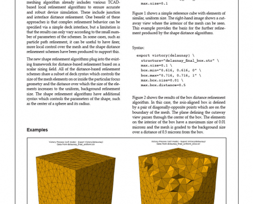 https://silvaco.com/wp-content/uploads/2020/03/simstd_Q3_2014_hints2.jpg
1012
782
Ingrid Schwarz
/wp-content/uploads/2019/11/silvaco-logo.png
Ingrid Schwarz2014-07-01 16:07:272021-10-13 10:21:04Hints, Tips, and Solutions – Types of 3D Delaunay Shape Refinement in Victory Process
https://silvaco.com/wp-content/uploads/2020/03/simstd_Q3_2014_hints2.jpg
1012
782
Ingrid Schwarz
/wp-content/uploads/2019/11/silvaco-logo.png
Ingrid Schwarz2014-07-01 16:07:272021-10-13 10:21:04Hints, Tips, and Solutions – Types of 3D Delaunay Shape Refinement in Victory Process