 https://silvaco.com/wp-content/uploads/2020/03/a1_Figure4a.jpg
508
550
Ingrid Schwarz
/wp-content/uploads/2019/11/silvaco-logo.png
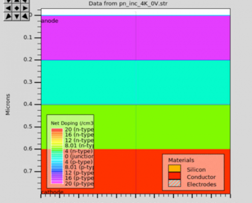
Ingrid Schwarz2018-04-01 23:42:042021-10-13 09:45:10TCAD Simulation of Si and GaAs p-n Junction Devices at Cryogenic Temperatures, Down to 2 K
https://silvaco.com/wp-content/uploads/2020/03/a1_Figure4a.jpg
508
550
Ingrid Schwarz
/wp-content/uploads/2019/11/silvaco-logo.png
Ingrid Schwarz2018-04-01 23:42:042021-10-13 09:45:10TCAD Simulation of Si and GaAs p-n Junction Devices at Cryogenic Temperatures, Down to 2 K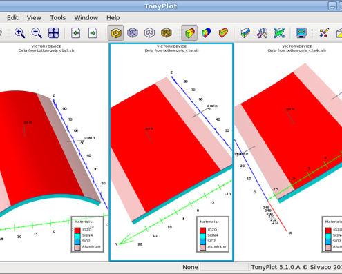 https://silvaco.com/wp-content/uploads/2020/03/bi-axial_fig2.jpg
397
550
Ingrid Schwarz
/wp-content/uploads/2019/11/silvaco-logo.png
Ingrid Schwarz2018-04-01 23:14:402021-10-13 09:45:10Bi-axial Deformation with Victory Mesh for Flexible Electronic Applications
https://silvaco.com/wp-content/uploads/2020/03/bi-axial_fig2.jpg
397
550
Ingrid Schwarz
/wp-content/uploads/2019/11/silvaco-logo.png
Ingrid Schwarz2018-04-01 23:14:402021-10-13 09:45:10Bi-axial Deformation with Victory Mesh for Flexible Electronic Applications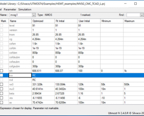 https://silvaco.com/wp-content/uploads/2020/03/a3_Fig2b.jpg
401
550
Ingrid Schwarz
/wp-content/uploads/2019/11/silvaco-logo.png
Ingrid Schwarz2018-04-01 22:17:382021-10-13 09:45:11TCAD-based GaN HEMT Scalable Modeling Flow Using the MVSG Compact Model
https://silvaco.com/wp-content/uploads/2020/03/a3_Fig2b.jpg
401
550
Ingrid Schwarz
/wp-content/uploads/2019/11/silvaco-logo.png
Ingrid Schwarz2018-04-01 22:17:382021-10-13 09:45:11TCAD-based GaN HEMT Scalable Modeling Flow Using the MVSG Compact Model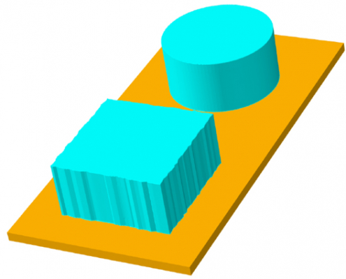 https://silvaco.com/wp-content/uploads/2020/03/hints-tips_fig3.jpg
426
550
Ingrid Schwarz
/wp-content/uploads/2019/11/silvaco-logo.png
Ingrid Schwarz2018-04-01 20:12:122021-10-13 09:45:11Hints, Tips and Solutions – Adding Random Noise to Mask Layout
https://silvaco.com/wp-content/uploads/2020/03/hints-tips_fig3.jpg
426
550
Ingrid Schwarz
/wp-content/uploads/2019/11/silvaco-logo.png
Ingrid Schwarz2018-04-01 20:12:122021-10-13 09:45:11Hints, Tips and Solutions – Adding Random Noise to Mask Layout https://silvaco.com/wp-content/uploads/2020/03/simstd_Q1_2018_a1-1.jpg
1012
782
Ingrid Schwarz
/wp-content/uploads/2019/11/silvaco-logo.png
Ingrid Schwarz2018-01-01 23:50:462021-10-13 09:48:22Advanced Process and Device 3D TCAD Simulation of Split-Gate Trench UMOSFET
https://silvaco.com/wp-content/uploads/2020/03/simstd_Q1_2018_a1-1.jpg
1012
782
Ingrid Schwarz
/wp-content/uploads/2019/11/silvaco-logo.png
Ingrid Schwarz2018-01-01 23:50:462021-10-13 09:48:22Advanced Process and Device 3D TCAD Simulation of Split-Gate Trench UMOSFET https://silvaco.com/wp-content/uploads/2020/03/simstd_Q1_2018_a2.jpg
1012
782
Ingrid Schwarz
/wp-content/uploads/2019/11/silvaco-logo.png
Ingrid Schwarz2018-01-01 23:02:332021-10-13 09:48:22Using TCAD to Reverse Engineer a 2N2222 BJT for Proton Damage Simulations
https://silvaco.com/wp-content/uploads/2020/03/simstd_Q1_2018_a2.jpg
1012
782
Ingrid Schwarz
/wp-content/uploads/2019/11/silvaco-logo.png
Ingrid Schwarz2018-01-01 23:02:332021-10-13 09:48:22Using TCAD to Reverse Engineer a 2N2222 BJT for Proton Damage Simulations https://silvaco.com/wp-content/uploads/2020/03/simstd_Q1_2018_a3.jpg
1012
782
Ingrid Schwarz
/wp-content/uploads/2019/11/silvaco-logo.png
Ingrid Schwarz2018-01-01 00:03:552021-10-13 09:48:22Optimization of PD-SOI CMOS Process and Devices for RF Applications
https://silvaco.com/wp-content/uploads/2020/03/simstd_Q1_2018_a3.jpg
1012
782
Ingrid Schwarz
/wp-content/uploads/2019/11/silvaco-logo.png
Ingrid Schwarz2018-01-01 00:03:552021-10-13 09:48:22Optimization of PD-SOI CMOS Process and Devices for RF Applications https://silvaco.com/wp-content/uploads/2020/03/simstd_Q4_2017_a4-1.jpg
1012
782
Ingrid Schwarz
/wp-content/uploads/2019/11/silvaco-logo.png
Ingrid Schwarz2017-10-01 22:18:522021-10-13 09:48:31W-element Field Solvers
https://silvaco.com/wp-content/uploads/2020/03/simstd_Q4_2017_a4-1.jpg
1012
782
Ingrid Schwarz
/wp-content/uploads/2019/11/silvaco-logo.png
Ingrid Schwarz2017-10-01 22:18:522021-10-13 09:48:31W-element Field Solvers https://silvaco.com/wp-content/uploads/2020/03/simstd_Q4_2017_a5-1.jpg
1012
782
Ingrid Schwarz
/wp-content/uploads/2019/11/silvaco-logo.png
Ingrid Schwarz2017-10-01 21:21:382021-10-13 09:48:31SmartSpice Shared Mode API
https://silvaco.com/wp-content/uploads/2020/03/simstd_Q4_2017_a5-1.jpg
1012
782
Ingrid Schwarz
/wp-content/uploads/2019/11/silvaco-logo.png
Ingrid Schwarz2017-10-01 21:21:382021-10-13 09:48:31SmartSpice Shared Mode API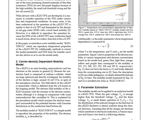 https://silvaco.com/wp-content/uploads/2020/03/simstd_Q4_2017_a3-1.jpg
1012
782
Ingrid Schwarz
/wp-content/uploads/2019/11/silvaco-logo.png
Ingrid Schwarz2017-10-01 00:03:552021-10-13 09:48:37Temperature Properties of Amorphous In-Ga-Zn-O Thin-Film Transistors with a new Mobility Model
https://silvaco.com/wp-content/uploads/2020/03/simstd_Q4_2017_a3-1.jpg
1012
782
Ingrid Schwarz
/wp-content/uploads/2019/11/silvaco-logo.png
Ingrid Schwarz2017-10-01 00:03:552021-10-13 09:48:37Temperature Properties of Amorphous In-Ga-Zn-O Thin-Film Transistors with a new Mobility Model