Simulation Standard
Technical Journal
A Journal for Process and Device Engineers
RFSOI Switch Harmonics Simulations with Trap-Rich Substrate
In this paper, in order to understand trap-rich substrate behavior, passive and active device on SOI with trap-rich layer structures were simulated using the Victory Device simulator. Harmonics distortion of devices were also compared.
Estimation of Interface Property Changes Between Normally On/Off Hydrogenated Diamond MISFETs
Introduction
Diamond is considered to be the ultimate semiconductor material for high power and high frequency devices due to its superior electrical and thermal properties, such as high breakdown field, high carrier mobility, low dielectric constant, and high thermal conductivity, as shown in Table 1.Furthermore, diamond has some unique electronic properties. The surface of diamond films terminated by hydrogen atoms has negative electron affinity (NEA) and can generate a two-dimensional hole accumulation layer suitable as a hole channel of a field-effect transistor.
TCAD Simulation of Electric Field Distribution in Gallium Nitride Trench-based Power Devices
IntroductionGallium nitride (GaN)-based devices are excellent candidates for high-voltage and high-power applications, due to the superior physical properties of GaN compared to Si, SiC, and GaAs. Recently, GaN vertical devices have attracted increased attention, due to their advantages over GaN lateral devices, including high breakdown voltage (BV) and current capability for a given chip size, and superior thermal performance.1 Recent demonstrations of high-performance vertical GaN diodes2–4 and transistors5–9 have made vertical structures very promising for GaN power devices.
Channel-length Dependence of a-IGZO TFTs with Self-heating Effects
IntroductionAmorphous In-Ga-Zn-O thin-film transistors (a-IGZO TFTs) show a high mobility, a small sub-threshold swing, and a low OFF-current, and they are considered to be one of the most promising TFT for new flat-panel displays (FPDs). The high mobility originates from the unique electron transport in a-IGZO. The transport properties are different from those in conventional semiconductor materials like Si, for example, the mobility increases with increase of the electron concentration and/or temperature. Therefore, the new mobility model for a-IGZO is necessary. In addition, as pixel sizes in the FPDs decreases, a channel-length, L, of a-IGZO TFTs becomes shorter. It indicates that it is important to understand the operation of short-channel a-IGZO TFTs.
Simulation of Different Tunnel Junctions in InGaP/GaAs, InGaP/CdTe Dual Junction Solar Cells
Abstract — Dual junction solar cells were simulated using Silvaco TCAD tool with various tunnel junction material compositions. InGaP/GaAs dual junction solar cells were simulated with 10 different tunnel junction combinations. The highest efficiencies were from InGaP/AlGaAs and InGaP/InGaP tunnel junctions at 31.82% and 31.75%. InGaP/CdTe solar cells were also simulated with four different tunnel junction combinations. InGaP/InGaP tunnel junction was found to be most efficient with 37.29% which is consistent with experimental data. Three of four InGaP/CdTe dual junction solar cells were simulated to have higher efficiency values than all InGaP/GaAs solar cells.
Hints, Tips and Solutions – July, August, September 2019
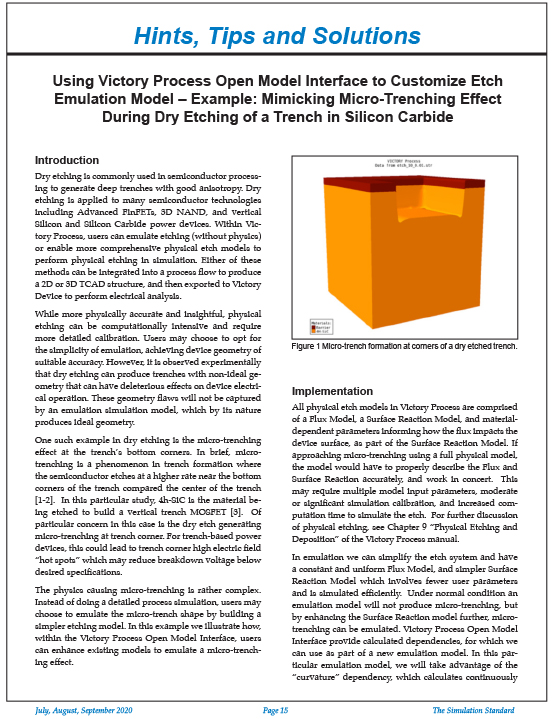
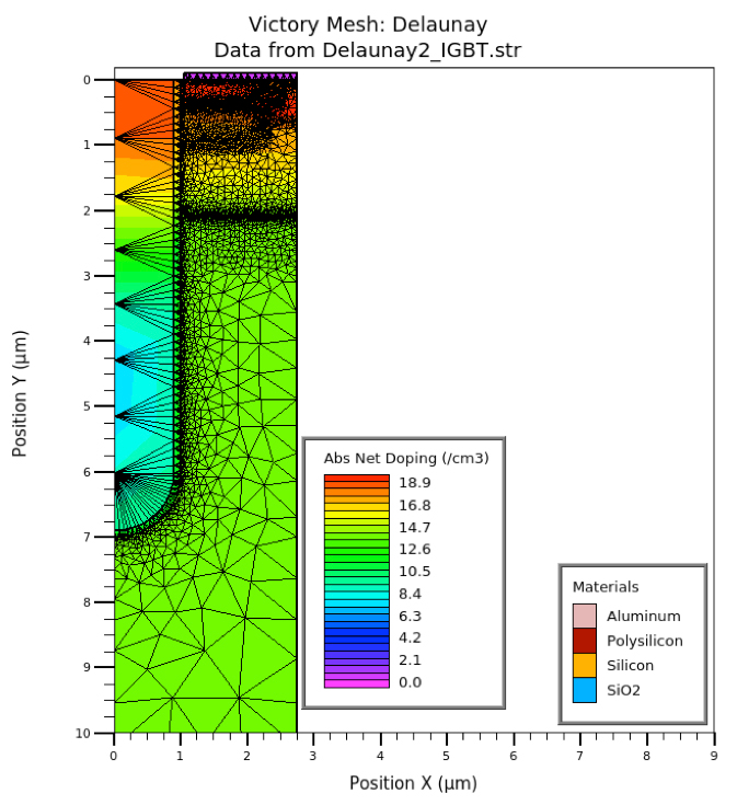
Q. Is it possible to emulate a deep reactive ion etch process (e.g. deep trench with scalloped sidewalls) without using a physical based process simulation, such as Victory Process?To study a non-ideal geometry and its impact on device performance, TCAD device engineers may want to generate structures with complex geometries quickly, without the added details of physically-based process simulation.