Simulation Standard
Technical Journal
A Journal for Process and Device Engineers
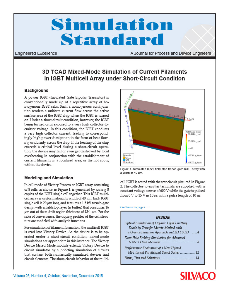
3D TCAD Mixed-Mode Simulation of Current Filaments in IGBT Multicell Array under Short-Circuit Condition
A power IGBT (Insulated Gate Bipolar Transistor) is conventionally made up of a repetitive array of homogenous IGBT cells. Such a homogenous configuration renders a uniform current flow across the active surface area of the IGBT chip when the IGBT is turned on. Under a short-circuit condition, however, the IGBT being turned on is exposed to a very high collector-to-emitter voltage. In this condition, the IGBT conducts a very high collector current, leading to correspondingly high power dissipation in the form of heat flowing uniformly across the chip. If the heating of the chip exceeds a critical level during a short-circuit operation, the device may fail or even get destroyed by local overheating in conjunction with the establishment of current filaments in a localized area, or the hot spots, within the device.
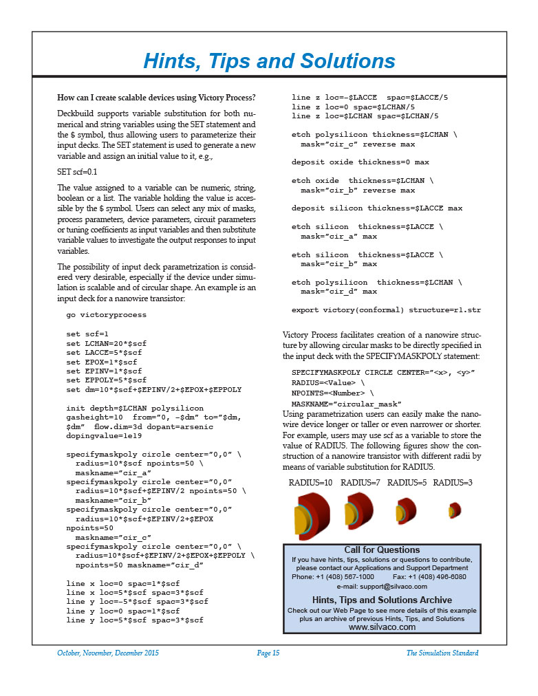
Hints, Tips and Solutions – Create scalable devices with Victory Process
Deckbuild supports variable substitution for both numerical and string variables using the SET statement and the $ symbol, thus allowing users to parameterize their input decks. The SET statement is used to generate a new variable and assign an initial value to it, e.g.,
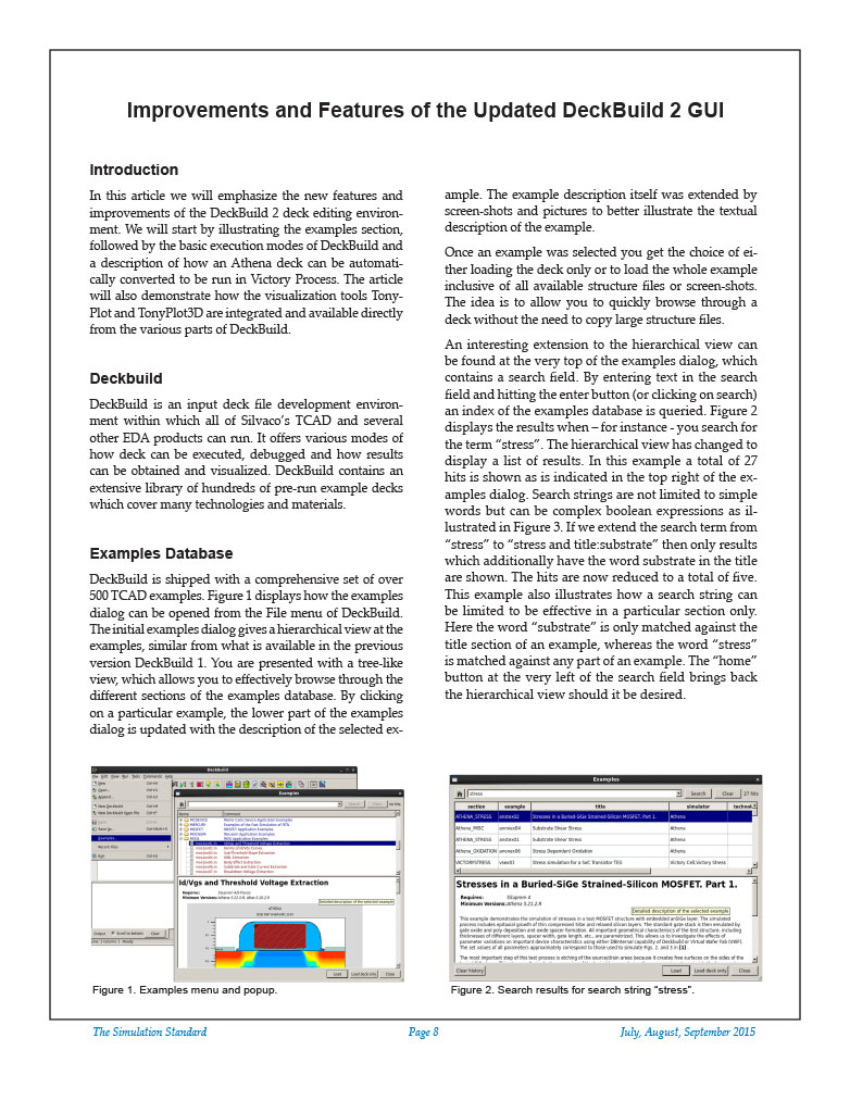
Improvements and Features of the Updated DeckBuild 2 GUI
In this article we will emphasize the new features and improvements of the DeckBuild 2 deck editing environment. We will start by illustrating the examples section, followed by the basic execution modes of DeckBuild and a description of how an Athena deck can be automatically converted to be run in Victory Process. The article will also demonstrate how the visualization tools TonyPlot and TonyPlot3D are integrated and available directly from the various parts of DeckBuild.
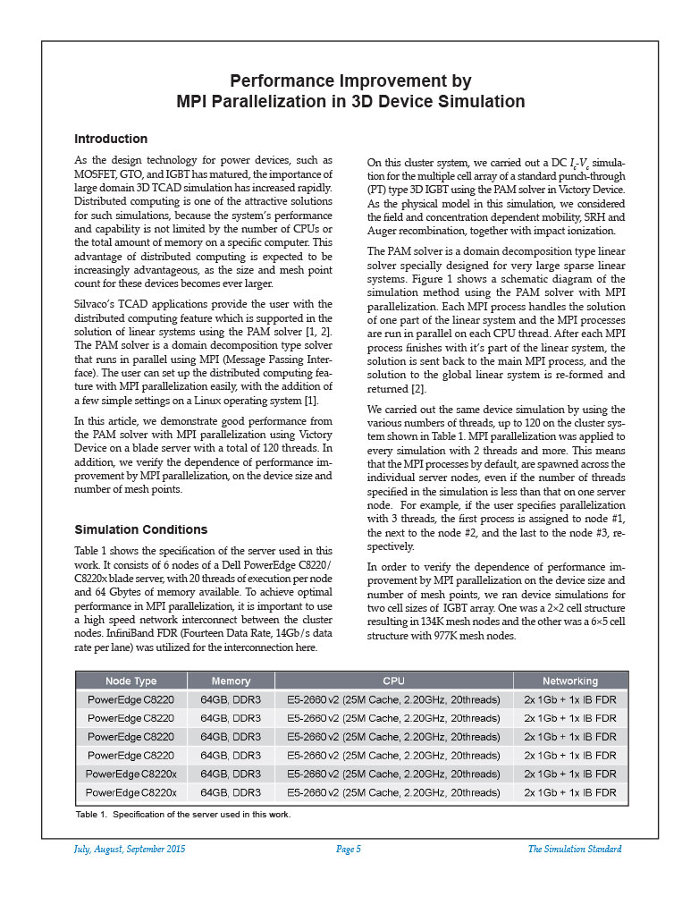
Performance Improvement by MPI Parallelization in 3D Device Simulation
As the design technology for power devices, such as MOSFET, GTO, and IGBT has matured, the importance of large domain 3D TCAD simulation has increased rapidly. Distributed computing is one of the attractive solutions for such simulations, because the system’s performance and capability is not limited by the number of CPUs or the total amount of memory on a specific computer. This advantage of distributed computing is expected to be increasingly advantageous, as the size and mesh point count for these devices becomes ever larger.
Electrical Simulation of Liquid Crystals
Liquid Crystals (LCs) are state of matter intermediate between that of a crystalline and a liquid. The optical, mechanical, electrical and magnetic properties of LC medium are defined by the orientation order of the constituent anisotropic molecules. Due to the anisotropy of the electrical properties, the orientation of the LC molecules is effectively controlled by electric fields. As a result, LCs exhibit very specific electrooptical phenomena because of their large birefringence. All of these are important to the functional devices based on LCs, for example, flat panel displays that have been commercialized for decades.
Hints, Tips and Solutions – Local conformal mesh refinement in Victory Process
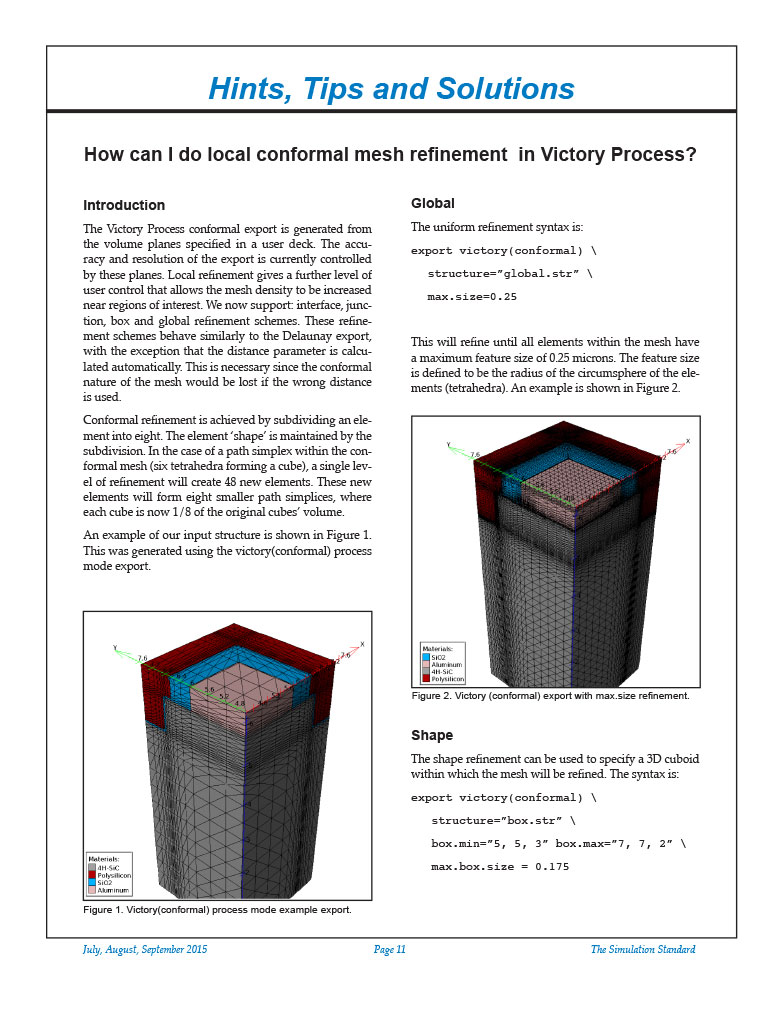
The Victory Process conformal export is generated from the volume planes specified in a user deck. The accuracy and resolution of the export is currently controlled by these planes. Local refinement gives a further level of user control that allows the mesh density to be increased near regions of interest. We now support: interface, junction, box and global refinement schemes. These refinement schemes behave similarly to the Delaunay export, with the exception that the distance parameter is calculated automatically. This is necessary since the conformal nature of the mesh would be lost if the wrong distance is used.

