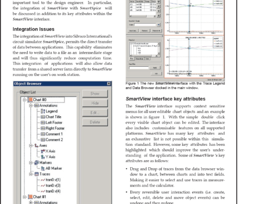
 https://silvaco.com/wp-content/uploads/simulationstandard/simstd_jan_2003_a3-e1611194908208.jpg
800
644
Graham Bell
/wp-content/uploads/2019/11/silvaco-logo.png
Graham Bell2003-01-01 21:57:532021-07-16 22:00:40SmartView – Integration Aspects and Key Attributes
https://silvaco.com/wp-content/uploads/simulationstandard/simstd_jan_2003_a3-e1611194908208.jpg
800
644
Graham Bell
/wp-content/uploads/2019/11/silvaco-logo.png
Graham Bell2003-01-01 21:57:532021-07-16 22:00:40SmartView – Integration Aspects and Key Attributes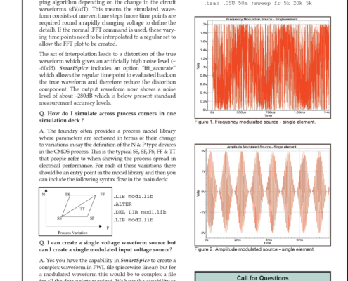 https://silvaco.com/wp-content/uploads/simulationstandard/simstd_jan_2003_hints-e1611193704223.jpg
800
644
Graham Bell
/wp-content/uploads/2019/11/silvaco-logo.png
Graham Bell2003-01-01 20:02:582021-07-16 22:00:41Getting an Accurate FFT Spectral Plot in SmartSpice
https://silvaco.com/wp-content/uploads/simulationstandard/simstd_jan_2003_hints-e1611193704223.jpg
800
644
Graham Bell
/wp-content/uploads/2019/11/silvaco-logo.png
Graham Bell2003-01-01 20:02:582021-07-16 22:00:41Getting an Accurate FFT Spectral Plot in SmartSpice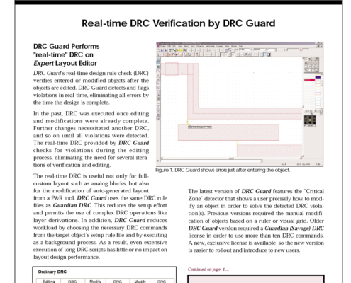 https://silvaco.com/wp-content/uploads/simulationstandard/simstd_dec_2002_a1.jpg
1669
1290
Graham Bell
/wp-content/uploads/2019/11/silvaco-logo.png
Graham Bell2002-12-01 23:03:162021-07-16 22:00:55Real-time DRC Verification by DRC Guard
https://silvaco.com/wp-content/uploads/simulationstandard/simstd_dec_2002_a1.jpg
1669
1290
Graham Bell
/wp-content/uploads/2019/11/silvaco-logo.png
Graham Bell2002-12-01 23:03:162021-07-16 22:00:55Real-time DRC Verification by DRC Guard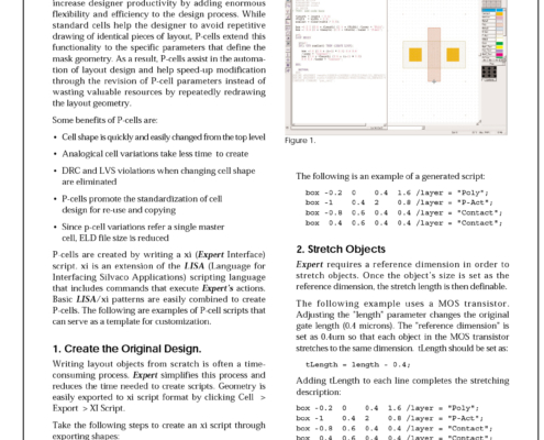 https://silvaco.com/wp-content/uploads/simulationstandard/simstd_dec_2002_a2.jpg
1669
1280
Graham Bell
/wp-content/uploads/2019/11/silvaco-logo.png
Graham Bell2002-12-01 22:06:502021-07-16 22:00:55Actual Examples of Creating Parameterized Cells
https://silvaco.com/wp-content/uploads/simulationstandard/simstd_dec_2002_a2.jpg
1669
1280
Graham Bell
/wp-content/uploads/2019/11/silvaco-logo.png
Graham Bell2002-12-01 22:06:502021-07-16 22:00:55Actual Examples of Creating Parameterized Cells https://silvaco.com/wp-content/uploads/simulationstandard/simstd_dec_2002_a3.jpg
1669
1281
Graham Bell
/wp-content/uploads/2019/11/silvaco-logo.png
Graham Bell2002-12-01 21:12:072021-07-16 22:00:56Connectivity Operations in Guardian DRC
https://silvaco.com/wp-content/uploads/simulationstandard/simstd_dec_2002_a3.jpg
1669
1281
Graham Bell
/wp-content/uploads/2019/11/silvaco-logo.png
Graham Bell2002-12-01 21:12:072021-07-16 22:00:56Connectivity Operations in Guardian DRC https://silvaco.com/wp-content/uploads/simulationstandard/simstd_dec_2002_hints.jpg
1669
1281
Graham Bell
/wp-content/uploads/2019/11/silvaco-logo.png
Graham Bell2002-12-01 17:19:472021-07-16 22:00:56How does Snap-to-grid Works for Cell Instances
https://silvaco.com/wp-content/uploads/simulationstandard/simstd_dec_2002_hints.jpg
1669
1281
Graham Bell
/wp-content/uploads/2019/11/silvaco-logo.png
Graham Bell2002-12-01 17:19:472021-07-16 22:00:56How does Snap-to-grid Works for Cell Instances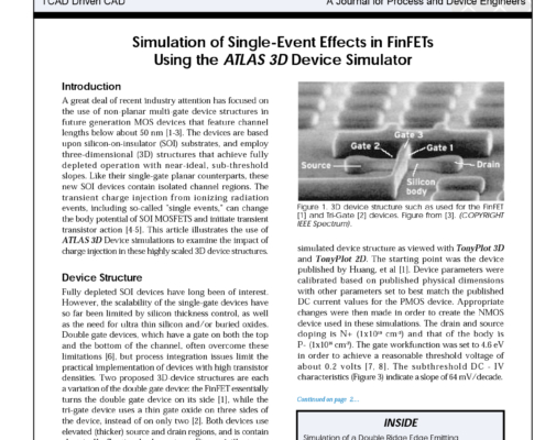 https://silvaco.com/wp-content/uploads/simulationstandard/simstd_nov_2002_a1.jpg
1669
1302
Graham Bell
/wp-content/uploads/2019/11/silvaco-logo.png
Graham Bell2002-11-01 23:25:262021-07-16 22:00:56Simulation of Single-Event Effects in FinFETs Using the ATLAS Device Simulator
https://silvaco.com/wp-content/uploads/simulationstandard/simstd_nov_2002_a1.jpg
1669
1302
Graham Bell
/wp-content/uploads/2019/11/silvaco-logo.png
Graham Bell2002-11-01 23:25:262021-07-16 22:00:56Simulation of Single-Event Effects in FinFETs Using the ATLAS Device Simulator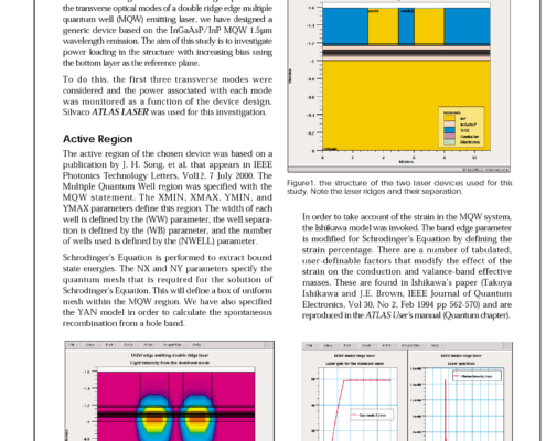 https://silvaco.com/wp-content/uploads/simulationstandard/simstd_nov_2002_a2.jpg
1669
1287
Graham Bell
/wp-content/uploads/2019/11/silvaco-logo.png
Graham Bell2002-11-01 22:36:452021-07-16 22:01:32Simulation of a Double Ridge Edge Emitting InGaAsP/InP MQW Laser
https://silvaco.com/wp-content/uploads/simulationstandard/simstd_nov_2002_a2.jpg
1669
1287
Graham Bell
/wp-content/uploads/2019/11/silvaco-logo.png
Graham Bell2002-11-01 22:36:452021-07-16 22:01:32Simulation of a Double Ridge Edge Emitting InGaAsP/InP MQW Laser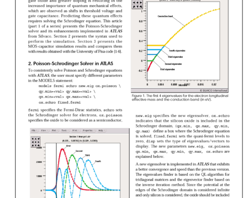 https://silvaco.com/wp-content/uploads/simulationstandard/simstd_nov_2002_a3.jpg
1669
1287
Graham Bell
/wp-content/uploads/2019/11/silvaco-logo.png
Graham Bell2002-11-01 21:43:302021-07-16 22:01:32Quantum Modeling Part I: Poisson-Schrodinger Solver
https://silvaco.com/wp-content/uploads/simulationstandard/simstd_nov_2002_a3.jpg
1669
1287
Graham Bell
/wp-content/uploads/2019/11/silvaco-logo.png
Graham Bell2002-11-01 21:43:302021-07-16 22:01:32Quantum Modeling Part I: Poisson-Schrodinger Solver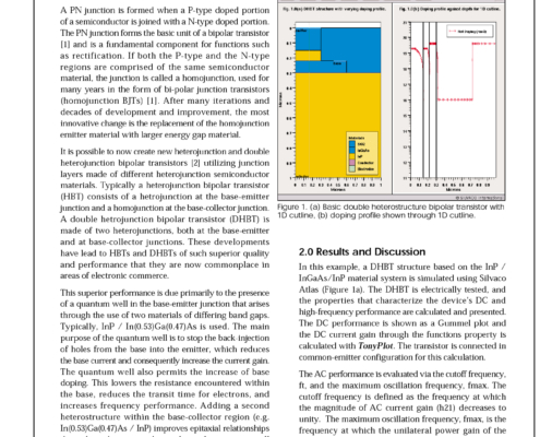 https://silvaco.com/wp-content/uploads/simulationstandard/simstd_nov_2002_a4-e1611194569487.jpg
800
616
Graham Bell
/wp-content/uploads/2019/11/silvaco-logo.png
Graham Bell2002-11-01 20:49:112021-07-16 22:01:33Simulation of a High Gain InP/InGaAs/InP Double HBT with Varying Doping Profile within ATLAS
https://silvaco.com/wp-content/uploads/simulationstandard/simstd_nov_2002_a4-e1611194569487.jpg
800
616
Graham Bell
/wp-content/uploads/2019/11/silvaco-logo.png
Graham Bell2002-11-01 20:49:112021-07-16 22:01:33Simulation of a High Gain InP/InGaAs/InP Double HBT with Varying Doping Profile within ATLAS