Simulation of Single-Event Effects in FinFETs Using the ATLAS Device Simulator
Introduction
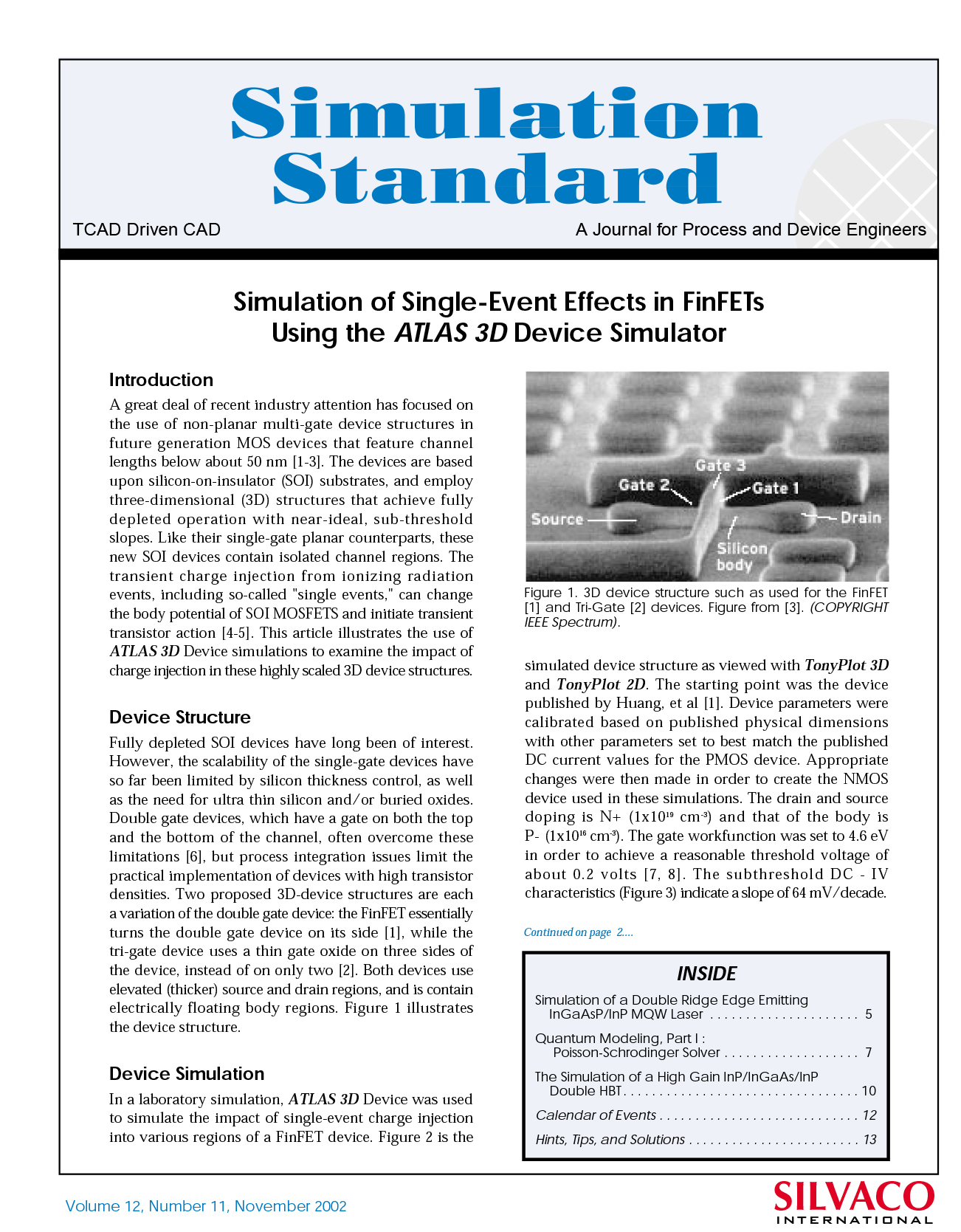
A great deal of recent industry attention has focused on the use of non-planar multi-gate device structures in future generation MOS devices that feature channel lengths below about 50 nm [1-3]. The devices are based upon silicon-on-insulator (SOI) substrates, and employ three-dimensional (3D) structures that achieve fully depleted operation with near-ideal, sub-threshold slopes. Like their single-gate planar counterparts, these new SOI devices contain isolated channel regions. The transient charge injection from ionizing radiation events, including so-called “single events,” can change the body potential of SOI MOSFETS and initiate transient transistor action [4-5]. This article illustrates the use of ATLAS Device simulations to examine the impact of charge injection in these highly scaled 3D device structures.


