TCAD Mixed-Mode Simulation for GaN Power HEMTs in Unclamped Inductive Switching
Introduction
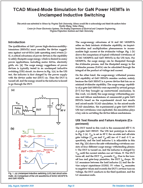
The qualification of GaN power high-electron-mobilitytransistors (HEMTs) must consider the device ruggedness against out-of-SOA (safe operating area) events [1- 3]. A critical robustness of power devices is the capability to safely dissipate surge energy, which is desired in many power applications, including motor drives, electricity grids, etc. [4]. The surge energy ruggedness of power devices is typically tested in an unclamped inductive switching (UIS) circuit. As shown in Fig. 1(a), in the UIS test, the inductor is first charged by the power supply with the device under test (DUT) on. Then the DUT is turned off, and the energy stored in the inductor is forced to go through the DUT. The surge-energy robustness of Si and SiC MOSFETs relies on their intrinsic avalanche capability, an impactionization and multiplication phenomenon to accommodate high current at the avalanche voltage. Fig. 1 (b) shows the comparison of typical withstand waveforms of Si/SiC MOSFETs and GaN HEMTs in the UIS tests. For MOSFETs, the surge energy can be dissipated through the avalanche process, and the dissipated energy in the avalanche process (EAVA) can be calculated through the integral of the product of voltage and current.
On the other hand, the surge-energy withstand process and capability of GaN HEMTs remains unclear, mainly because the GaN HEMT is a power device that has no or minimal avalanche capability. The surge energy capability of p-gate GaN HEMTs were reported by several groups [5-7] but they brought up controversial conclusions. In this work, we clarify the surge energy withstanding process and failure mechanisms of commercial p-gate GaN HEMTs based on the experimental circuit test results and mixed-mode TCAD simulation. In the mixed-mode TCAD simulation, the experimental p-gate GaN HEMT UIS test waveforms were replicated, the simulation plays a key role in unveiling the device failure mechanisms.


