
Simulation Standard
Technical Journal
A Journal for Process and Device Engineers
 https://silvaco.com/wp-content/uploads/2020/02/simstd_Q1_2017_a2.jpg
1012
782
Ingrid Schwarz
/wp-content/uploads/2019/11/silvaco-logo.png
Ingrid Schwarz2017-01-01 17:44:512021-07-16 21:38:15Simulation of a Bipolar Junction Transistor Under High and Low Current Injection Conditions
https://silvaco.com/wp-content/uploads/2020/02/simstd_Q1_2017_a2.jpg
1012
782
Ingrid Schwarz
/wp-content/uploads/2019/11/silvaco-logo.png
Ingrid Schwarz2017-01-01 17:44:512021-07-16 21:38:15Simulation of a Bipolar Junction Transistor Under High and Low Current Injection Conditions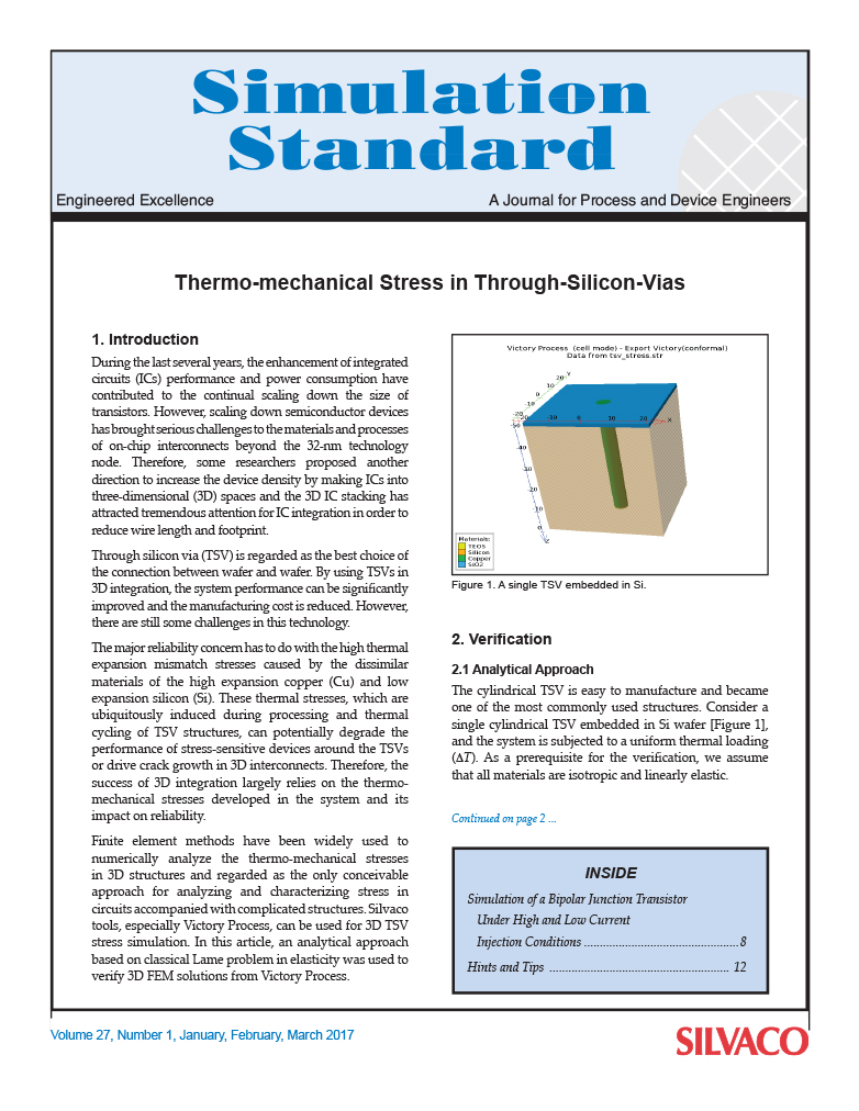 https://silvaco.com/wp-content/uploads/2020/02/simstd_Q1_2017_a1.jpg
1012
782
Ingrid Schwarz
/wp-content/uploads/2019/11/silvaco-logo.png
Ingrid Schwarz2017-01-01 17:41:142021-07-16 21:38:15Thermo-mechanical Stress in Through-Silicon-Vias
https://silvaco.com/wp-content/uploads/2020/02/simstd_Q1_2017_a1.jpg
1012
782
Ingrid Schwarz
/wp-content/uploads/2019/11/silvaco-logo.png
Ingrid Schwarz2017-01-01 17:41:142021-07-16 21:38:15Thermo-mechanical Stress in Through-Silicon-Vias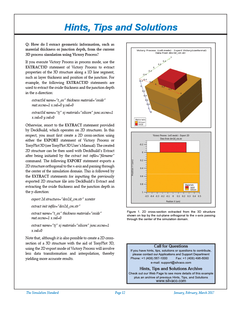 https://silvaco.com/wp-content/uploads/2020/02/simstd_Q1_2017_hints.jpg
1012
782
Ingrid Schwarz
/wp-content/uploads/2019/11/silvaco-logo.png
Ingrid Schwarz2017-01-01 10:59:252021-07-16 21:38:16Hints, Tips and Solutions – Extract geometric information from 3D process simulation
https://silvaco.com/wp-content/uploads/2020/02/simstd_Q1_2017_hints.jpg
1012
782
Ingrid Schwarz
/wp-content/uploads/2019/11/silvaco-logo.png
Ingrid Schwarz2017-01-01 10:59:252021-07-16 21:38:16Hints, Tips and Solutions – Extract geometric information from 3D process simulation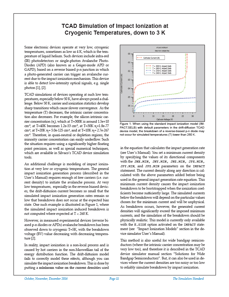 https://silvaco.com/wp-content/uploads/2020/03/simstd_Q4_2016_a3-1.jpg
1012
782
Ingrid Schwarz
/wp-content/uploads/2019/11/silvaco-logo.png
Ingrid Schwarz2016-10-01 20:44:512021-07-16 21:38:30TCAD Simulation of Impact Ionization at Cryogenic Temperatures, down to 3 K
https://silvaco.com/wp-content/uploads/2020/03/simstd_Q4_2016_a3-1.jpg
1012
782
Ingrid Schwarz
/wp-content/uploads/2019/11/silvaco-logo.png
Ingrid Schwarz2016-10-01 20:44:512021-07-16 21:38:30TCAD Simulation of Impact Ionization at Cryogenic Temperatures, down to 3 K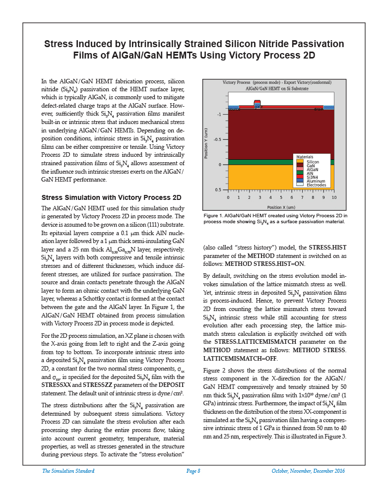 https://silvaco.com/wp-content/uploads/2020/03/simstd_Q4_2016_a2-1.jpg
1012
782
Ingrid Schwarz
/wp-content/uploads/2019/11/silvaco-logo.png
Ingrid Schwarz2016-10-01 20:42:032021-07-16 21:38:30Stress Induced by Intrinsically Strained Silicon Nitride Passivation Films of AlGaN/GaN HEMTs Using Victory Process 2D
https://silvaco.com/wp-content/uploads/2020/03/simstd_Q4_2016_a2-1.jpg
1012
782
Ingrid Schwarz
/wp-content/uploads/2019/11/silvaco-logo.png
Ingrid Schwarz2016-10-01 20:42:032021-07-16 21:38:30Stress Induced by Intrinsically Strained Silicon Nitride Passivation Films of AlGaN/GaN HEMTs Using Victory Process 2D https://silvaco.com/wp-content/uploads/2020/03/simstd_Q4_2016_a1-1.jpg
1012
782
Ingrid Schwarz
/wp-content/uploads/2019/11/silvaco-logo.png
Ingrid Schwarz2016-10-01 19:15:132021-07-16 21:38:30Victory Process 2D – A Valuable Alternative To SUPREM-based Simulators
https://silvaco.com/wp-content/uploads/2020/03/simstd_Q4_2016_a1-1.jpg
1012
782
Ingrid Schwarz
/wp-content/uploads/2019/11/silvaco-logo.png
Ingrid Schwarz2016-10-01 19:15:132021-07-16 21:38:30Victory Process 2D – A Valuable Alternative To SUPREM-based Simulators