
Simulation Standard
Technical Journal
A Journal for Process and Device Engineers
 https://silvaco.com/wp-content/uploads/2020/03/a3_Fig2b.jpg
401
550
Ingrid Schwarz
/wp-content/uploads/2019/11/silvaco-logo.png
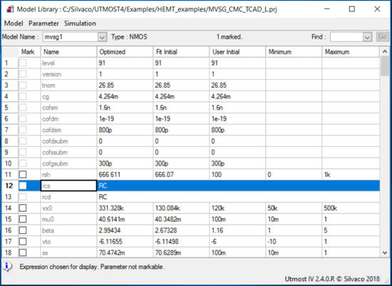
Ingrid Schwarz2018-04-01 22:17:382021-07-16 21:36:11TCAD-based GaN HEMT Scalable Modeling Flow Using the MVSG Compact Model
https://silvaco.com/wp-content/uploads/2020/03/a3_Fig2b.jpg
401
550
Ingrid Schwarz
/wp-content/uploads/2019/11/silvaco-logo.png
Ingrid Schwarz2018-04-01 22:17:382021-07-16 21:36:11TCAD-based GaN HEMT Scalable Modeling Flow Using the MVSG Compact Model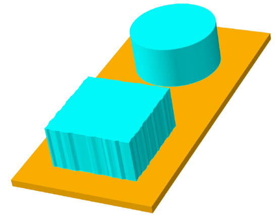 https://silvaco.com/wp-content/uploads/2020/03/hints-tips_fig3.jpg
426
550
Ingrid Schwarz
/wp-content/uploads/2019/11/silvaco-logo.png
Ingrid Schwarz2018-04-01 20:12:122021-07-16 21:36:25Hints, Tips and Solutions – Adding Random Noise to Mask Layout
https://silvaco.com/wp-content/uploads/2020/03/hints-tips_fig3.jpg
426
550
Ingrid Schwarz
/wp-content/uploads/2019/11/silvaco-logo.png
Ingrid Schwarz2018-04-01 20:12:122021-07-16 21:36:25Hints, Tips and Solutions – Adding Random Noise to Mask Layout https://silvaco.com/wp-content/uploads/2020/03/simstd_Q1_2018_a1-1.jpg
1012
782
Ingrid Schwarz
/wp-content/uploads/2019/11/silvaco-logo.png
Ingrid Schwarz2018-01-01 23:50:462021-07-16 21:36:25Advanced Process and Device 3D TCAD Simulation of Split-Gate Trench UMOSFET
https://silvaco.com/wp-content/uploads/2020/03/simstd_Q1_2018_a1-1.jpg
1012
782
Ingrid Schwarz
/wp-content/uploads/2019/11/silvaco-logo.png
Ingrid Schwarz2018-01-01 23:50:462021-07-16 21:36:25Advanced Process and Device 3D TCAD Simulation of Split-Gate Trench UMOSFET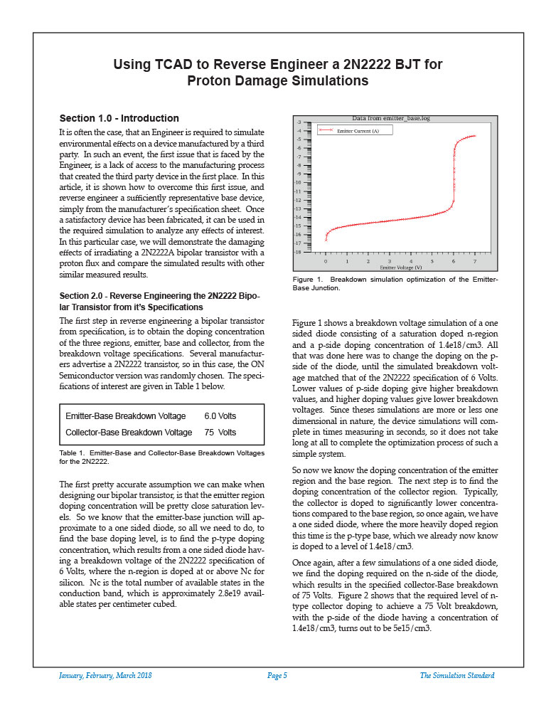 https://silvaco.com/wp-content/uploads/2020/03/simstd_Q1_2018_a2.jpg
1012
782
Ingrid Schwarz
/wp-content/uploads/2019/11/silvaco-logo.png
Ingrid Schwarz2018-01-01 23:02:332021-07-16 21:36:26Using TCAD to Reverse Engineer a 2N2222 BJT for Proton Damage Simulations
https://silvaco.com/wp-content/uploads/2020/03/simstd_Q1_2018_a2.jpg
1012
782
Ingrid Schwarz
/wp-content/uploads/2019/11/silvaco-logo.png
Ingrid Schwarz2018-01-01 23:02:332021-07-16 21:36:26Using TCAD to Reverse Engineer a 2N2222 BJT for Proton Damage Simulations https://silvaco.com/wp-content/uploads/2020/03/simstd_Q1_2018_a3.jpg
1012
782
Ingrid Schwarz
/wp-content/uploads/2019/11/silvaco-logo.png
Ingrid Schwarz2018-01-01 00:03:552021-07-16 21:36:26Optimization of PD-SOI CMOS Process and Devices for RF Applications
https://silvaco.com/wp-content/uploads/2020/03/simstd_Q1_2018_a3.jpg
1012
782
Ingrid Schwarz
/wp-content/uploads/2019/11/silvaco-logo.png
Ingrid Schwarz2018-01-01 00:03:552021-07-16 21:36:26Optimization of PD-SOI CMOS Process and Devices for RF Applications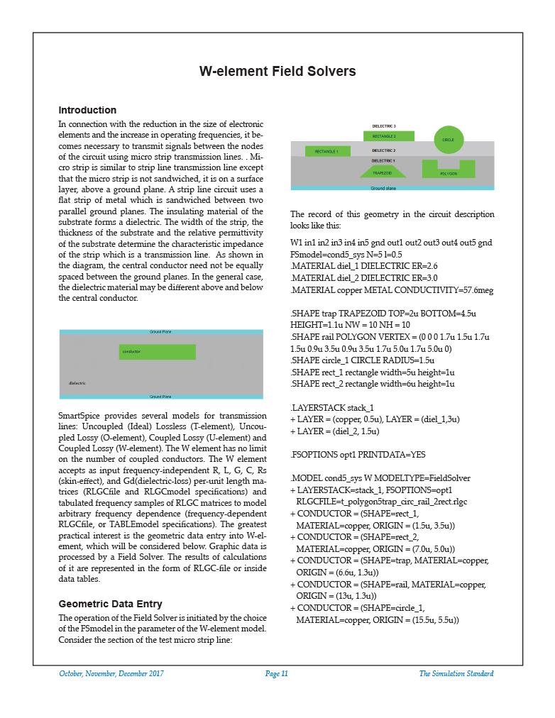 https://silvaco.com/wp-content/uploads/2020/03/simstd_Q4_2017_a4-1.jpg
1012
782
Ingrid Schwarz
/wp-content/uploads/2019/11/silvaco-logo.png
Ingrid Schwarz2017-10-01 22:18:522021-07-16 21:36:26W-element Field Solvers
https://silvaco.com/wp-content/uploads/2020/03/simstd_Q4_2017_a4-1.jpg
1012
782
Ingrid Schwarz
/wp-content/uploads/2019/11/silvaco-logo.png
Ingrid Schwarz2017-10-01 22:18:522021-07-16 21:36:26W-element Field Solvers