Simulation Standard
Technical Journal
A Journal for Process and Device Engineers
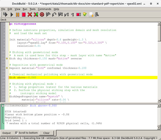
Hints, Tips and Solutions – Movie and PDF Report Generation with the DeckBuild GUI
Introduction
In this article we will emphasize two new features of the DeckBuild deck editing environment. These are the movie creation on the one hand and the creation of PDF reports on the other. The latest version of DeckBuild allows you to use recorded history points to prepare movies and PDF reports of a simulation flow. We will start by first illustrating the basic history creation and script execution mechanism, followed by pointing out the creation of movies. After that, we will demonstrate how to create a customized PDF report out of your simulation flow.

Process Variation, Alignment and BEOL Effects on Circuit Level Performance
As process nodes continue to shrink, the requirement for additional physics is gradually creeping into each stage of the design process. By way of illustration, TCAD simulations are becoming more atomistic in nature, SPICE models are becoming process-aware to take account of localized strain effects, and back or middle end of line (BEOL and MEOL) parasitics are moving from exclusively 2D rule based solutions to full 3D structure field solvers for numerous critical sections of the layout.
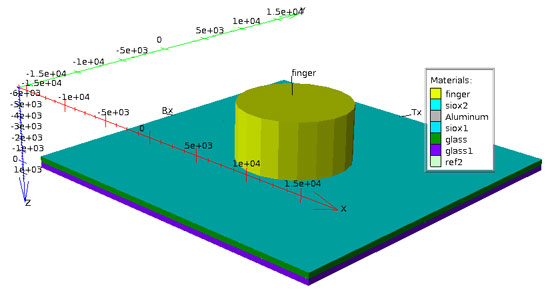
Touch Panel Capacitance Extraction in Hipex Full Chip Extraction Tool Using Stellar Field Solver
The previously standalone Stellar GUI based field solver tool for parasitic extraction is now integrated into Hipex (Silvaco’s full chip extraction tool) in Expert GUI. In Hipex, user can choose proper extraction method (including Steller solver) among different approaches. The GUI of Expert (Silvaco’s layout editor) has been extended to provide technology setup for Stellar mode of Hipex. Also, Expert provides full functional features of GDS drawing, editing and rule checking. As opposed to the Clever field solver based on adaptive meshing, Stellar can handle very large layout size with less memory and reduced runtime with acceptable accuracy (as compared to Clever). Clever, as very accurate adaptive meshing field solver, can be used as reference accuracy check when Stellar or rule based parasitic extraction method is performed in Hipex. In this article, we will review the basic interface of Hipex in Expert GUI using Stellar as a field solver to extract capacitance in touch panel example.
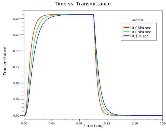
Dynamic Analysis of Liquid Crystal Pixels
We have demonstrated in previous articles the static electrical and optical simulation of LC cells [1][2]. The last piece of the function for a comprehensive analysis of an LC pixel is the capability of performing transient simulation. In this article, we will show the dynamic calculation of the LC director and the combination of electrical and optical simulation.
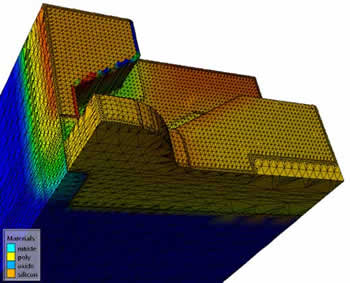
Hints, Tips and Solutions – Adding An Impurity to a Diffusion Model and Enable Diffusion of a New Impurity in a Specific Material
OBJECTIVE
Add an impurity (H) to a material (silicon) for a diffusion model (Fermi).
The description below refers to Victory Process version 7.27.X.
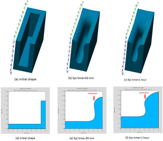
3D Topography Simulation of SiC Epitaxial Growth Modeled by Diffusive Flux and Gibbs-Thomson Effect
One of wide bandgap semiconductors, SiC has been widely applied to the power devices, and then, the super-junction MOS transistor of SiC is being investigated to obtain higher performance for Ron and BV [1]. The super-junction structure is fabricated by trench filling with the epitaxial growth [2, 3].

