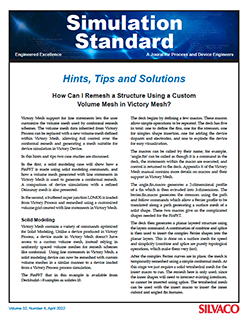
How Can I Remesh a Structure Using a Custom Volume Mesh in Victory Mesh?
Victory Mesh support for line statements lets the user customize the volume mesh used by conformal remesh schemes. The volume mesh data inherited from Victory Process can be replaced with a new volume mesh defined within Victory Mesh, allowing full control over the conformal remesh and generating a mesh suitable for device simulation in Victory Device.
In this hints and tips two case studies are discussed.
In the first, a solid modeling case will show how a FinFET is made using solid modeling commands, and how a volume mesh generated with line statements in Victory Mesh is used to generate a conformal remesh. A comparison of device simulations with a refined Delaunay mesh is also presented.
In the second, a buffered super junction LDMOS is loaded from Victory Process and remeshed using a customized volume grid created with line statements in Victory Mesh.
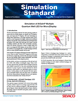
Simulation of AlGaInP Multiple Quantum Well LED for Micro Display
The flat panel display industry has been growing rapidly for recent years in mobile display, car display, AR/VR applications, and large-scale TVs display. The core technology enabling these applications is the light emitting diode (LED), which is a key component to realize the highly visible, power efficient, displays. For decades, many researchers have developed blue and green LEDs using wide band gap GaN-based wurtzite crystalline material, and successfully manufactured LED devices. However, to make a bright white LED and/or an integrated RGB display, red and yellow LED is also needed. To accomplish this, a smaller bandgap material like a cubic AlGaInP material can be used.
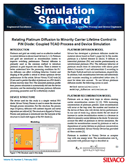
Relating Platinum Diffusion to Minority Carrier Lifetime Control in PiN Diode: Coupled TCAD Process and Device Simulation
Platinum and gold are widely used as an effective method to control lifetime in silicon-based devices [1, 2, 3]. Platinum and gold are introduced as recombination centers to improve switching performance. Thermal diffusion is primarily used as the common method to introduce platinum or gold dopants into silicon. There is interest to better understand how the processing conditions for Pt/Au diffusion can affect switching behavior. Control and shaping of the profile is critical to obtain optimum device performance. In this article, Silvaco Victory TCAD tools [4] [5] are used to predict the effect of platinum on a PiN diode’s reverse recovery time (Trr). The simulated platinum profile from process simulation is automatically fed into the device simulator, and the relationship between platinum diffusion processing parameters and Trr is effortlessly studied.
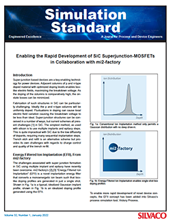
Enabling the Rapid Development of SiC Superjunction-MOSFETs in Collaboration with mi2-factory
Introduction
Super-junction based devices are a key enabling technology for power devices. Adjacent columns of p and n-type doped material with optimized doping levels enables box-like electric fields, maximizing the breakdown voltage. As the doping of the columns is comparatively high, the on-state losses can be minimized.
Fabrication of such structures in SiC can be particularly challenging. Ideally the p and n-type columns will be uniformly doped. Fluctuations in doping can cause local electric field variation causing the breakdown voltage to be less than ideal. Super-junction structures can be conceived in a number of ways, but current schemes all present challenges [1] in SiC. The simplest method, as used with silicon is to use multiple implants and epitaxy steps. This is quite impractical with SiC due to the low diffusivity of dopants, requiring many sequential implantation steps. Trench etch and refill is an alternative scheme but provides its own challenges with regards to charge control and quality of the trench re-fill.
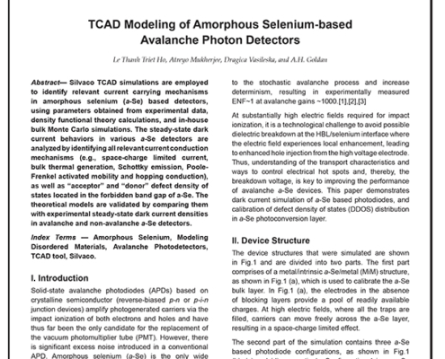
TCAD Modeling of Amorphous Selenium-based Avalanche Photon Detectors
Abstract— Silvaco TCAD simulations are employed to identify relevant current carrying mechanisms in amorphous selenium (a-Se) based detectors, using parameters obtained from experimental data, density functional theory calculations, and in-house bulk Monte Carlo simulations. The steady-state dark current behaviors in various a-Se detectors are analyzed by identifying all relevant current conduction mechanisms (e.g., space-charge limited current, bulk thermal generation, Schottky emission, Poole-Frenkel activated mobility and hopping conduction), as well as “acceptor” and “donor” defect density of states located in the forbidden band gap of a-Se. The theoretical models are validated by comparing them with experimental steady-state dark current densities in avalanche and non-avalanche a-Se detectors.
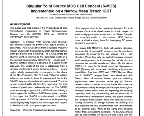
Singular Point Source MOS Cell Concept (S-MOS) Implemented on a Narrow Mesa Trench IGBT
Abstract— A Singular Point Source MOS (S-MOS) cell concept suitable for power MOS based devices is presented. The S-MOS differs from a standard Planar or Trench MOS cell in the manner by which the total channel width per device area is devised. The S-MOS single cell channel width is defined as the peripheral length of a line running approximately along the N++ source and P channel junction which is positioned on a gated trench side-wall. The length of the line is established from a singular point implant source for forming the N++ source region which geometrically corresponds to the shape of the N++/P junction. The N++ and PChannel profiles achieved are similar to those for a planar cell, but for the S-MOS, they are situated on a trench side-wall. The total device channel width will therefore depend on the total number of gated trench side-walls per chip. The S-MOS provides a unique approach for MOS cell layout designs and is applicable to different MOS based power devices. In this paper, the S-MOS is implemented on a 1200V IGBT by means of 3D-TCAD simulations while providing results highlighting the potential advantages with respect to the device static and dynamic performance.
Keywords – MOS cell, Insulated gate bipolar transistors.
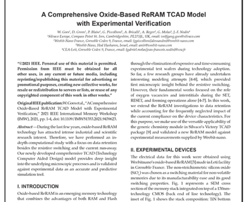
A Comprehensive Oxide-Based ReRAM TCAD Model with Experimental Verification
Abstract—During the last few years, oxide-based ReRAM technology has attracted intense industrial and scientific research interest. Therefore, we have performed an in-depth computational study with a focus on data retention besides the resistive switching and the current run-away. Our newly developed comprehensive TCAD (Technology Computer Aided Design) model provides deep insight into the underlying microscopic processes and is validated against experimental data as an accurate and predictive simulation tool.
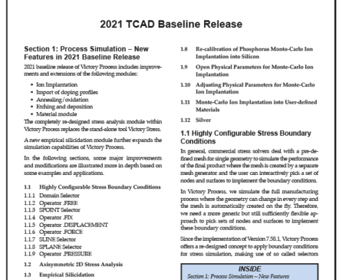
2021 TCAD Baseline Release
New Features in 2021 Baseline Release:
- Section 1: Process Simulation
- Section 2: Device Simulation
- Section 3: Victory Mesh
- Section 4: Parasitic Extraction

An Introduction to Meshing in Victory Process
Victory Process (VP) uses two types of mesh to represent the structure:
• The geometry mesh, which is used to represent the material regions.
• The volume mesh, which is used to represent the volume data (doping etc).
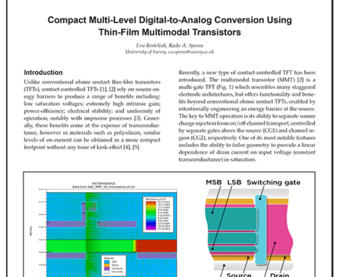
Compact Multi-Level Digital-to-Analog Conversion Using Thin-Film Multimodal Transistors
Unlike conventional ohmic contact thin-film transistors (TFTs), contact-controlled TFTs [1], [2] rely on source energy barriers to produce a range of benefits including: low saturation voltages; extremely high intrinsic gain; power-efficiency; electrical stability; and uniformity of operation, notably with imprecise processes [3]. Generally, these benefits come at the expense of transconductance, however in materials such as polysilicon, similar levels of on-current can be obtained in a more compact footprint without any trace of kink-effect [4], [5].
