 https://silvaco.com/wp-content/uploads/2021/06/simstd_Jun_2021_a1.jpg
767
600
Gigi Boss
/wp-content/uploads/2019/11/silvaco-logo.png
Gigi Boss2021-06-15 12:46:272021-07-16 21:31:32An Introduction to Meshing in Victory Process
https://silvaco.com/wp-content/uploads/2021/06/simstd_Jun_2021_a1.jpg
767
600
Gigi Boss
/wp-content/uploads/2019/11/silvaco-logo.png
Gigi Boss2021-06-15 12:46:272021-07-16 21:31:32An Introduction to Meshing in Victory Process https://silvaco.com/wp-content/uploads/2021/05/Q2_SS_May2021.jpg
766
600
Gigi Boss
/wp-content/uploads/2019/11/silvaco-logo.png
Gigi Boss2021-05-21 17:02:332021-07-16 21:31:32Compact Multi-Level Digital-to-Analog Conversion Using Thin-Film Multimodal Transistors
https://silvaco.com/wp-content/uploads/2021/05/Q2_SS_May2021.jpg
766
600
Gigi Boss
/wp-content/uploads/2019/11/silvaco-logo.png
Gigi Boss2021-05-21 17:02:332021-07-16 21:31:32Compact Multi-Level Digital-to-Analog Conversion Using Thin-Film Multimodal Transistors https://silvaco.com/wp-content/uploads/2021/04/simstd_April_2021_a1.jpg
766
600
Gigi Boss
/wp-content/uploads/2019/11/silvaco-logo.png
Gigi Boss2021-04-19 11:11:392021-07-16 21:31:33Investigation and Explanation of PiPiN Avalanche Photo-Diode Characteristics
https://silvaco.com/wp-content/uploads/2021/04/simstd_April_2021_a1.jpg
766
600
Gigi Boss
/wp-content/uploads/2019/11/silvaco-logo.png
Gigi Boss2021-04-19 11:11:392021-07-16 21:31:33Investigation and Explanation of PiPiN Avalanche Photo-Diode Characteristics https://silvaco.com/wp-content/uploads/2021/03/Q1_SS_Mar2021-1.png
724
567
Erick Castellon
/wp-content/uploads/2019/11/silvaco-logo.png
Erick Castellon2021-03-04 16:21:142021-07-16 21:31:33How do I create complex shapes with fixed cross sections in Victory Mesh?
https://silvaco.com/wp-content/uploads/2021/03/Q1_SS_Mar2021-1.png
724
567
Erick Castellon
/wp-content/uploads/2019/11/silvaco-logo.png
Erick Castellon2021-03-04 16:21:142021-07-16 21:31:33How do I create complex shapes with fixed cross sections in Victory Mesh? https://silvaco.com/wp-content/uploads/2021/02/simstd_feb_2021_a1.jpg
600
470
Erick Castellon
/wp-content/uploads/2019/11/silvaco-logo.png
Erick Castellon2021-02-03 19:16:132021-07-16 21:31:34Parabolic Grading of a PHEMT Channel Composition for Ultra-High and Broad OIP3 Peak
https://silvaco.com/wp-content/uploads/2021/02/simstd_feb_2021_a1.jpg
600
470
Erick Castellon
/wp-content/uploads/2019/11/silvaco-logo.png
Erick Castellon2021-02-03 19:16:132021-07-16 21:31:34Parabolic Grading of a PHEMT Channel Composition for Ultra-High and Broad OIP3 Peak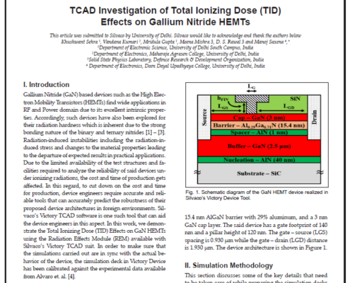 https://silvaco.com/wp-content/uploads/2021/01/simstd_jan_2021_a1.png
875
668
Graham Bell
/wp-content/uploads/2019/11/silvaco-logo.png
Graham Bell2021-01-04 12:04:432021-07-16 21:31:48TCAD Investigation of Total Ionizing Dose (TID) Effects on Gallium Nitride HEMTs
https://silvaco.com/wp-content/uploads/2021/01/simstd_jan_2021_a1.png
875
668
Graham Bell
/wp-content/uploads/2019/11/silvaco-logo.png
Graham Bell2021-01-04 12:04:432021-07-16 21:31:48TCAD Investigation of Total Ionizing Dose (TID) Effects on Gallium Nitride HEMTs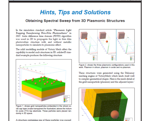 https://silvaco.com/wp-content/uploads/2020/12/simstd_dec_2020_a4.png
909
703
Graham Bell
/wp-content/uploads/2019/11/silvaco-logo.png
Graham Bell2020-12-02 10:31:342021-07-16 21:31:54Obtaining Spectral Sweeps from 3D Plasmonic Structures
https://silvaco.com/wp-content/uploads/2020/12/simstd_dec_2020_a4.png
909
703
Graham Bell
/wp-content/uploads/2019/11/silvaco-logo.png
Graham Bell2020-12-02 10:31:342021-07-16 21:31:54Obtaining Spectral Sweeps from 3D Plasmonic Structures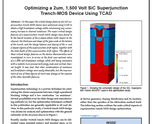 https://silvaco.com/wp-content/uploads/2020/10/simstd_Q3_2020_a1.jpg
724
567
Erick Castellon
/wp-content/uploads/2019/11/silvaco-logo.png
Erick Castellon2020-10-01 00:05:322021-07-16 21:31:54Optimizing a 2um, 1,500 Volt SiC Superjunction Trench-MOS Device Using TCAD
https://silvaco.com/wp-content/uploads/2020/10/simstd_Q3_2020_a1.jpg
724
567
Erick Castellon
/wp-content/uploads/2019/11/silvaco-logo.png
Erick Castellon2020-10-01 00:05:322021-07-16 21:31:54Optimizing a 2um, 1,500 Volt SiC Superjunction Trench-MOS Device Using TCAD https://silvaco.com/wp-content/uploads/2020/10/simstd_Q3_2020_a2.jpg
719
546
Erick Castellon
/wp-content/uploads/2019/11/silvaco-logo.png
Erick Castellon2020-10-01 00:04:372021-07-16 21:31:55TCAD Simulation of CBRAM Devices
https://silvaco.com/wp-content/uploads/2020/10/simstd_Q3_2020_a2.jpg
719
546
Erick Castellon
/wp-content/uploads/2019/11/silvaco-logo.png
Erick Castellon2020-10-01 00:04:372021-07-16 21:31:55TCAD Simulation of CBRAM Devices https://silvaco.com/wp-content/uploads/2020/10/simstd_Q3_2020_a3.jpg
719
546
Erick Castellon
/wp-content/uploads/2019/11/silvaco-logo.png
Erick Castellon2020-10-01 00:03:042021-07-16 21:31:55TCAD Mixed-Mode Simulation for GaN Power HEMTs in Unclamped Inductive Switching
https://silvaco.com/wp-content/uploads/2020/10/simstd_Q3_2020_a3.jpg
719
546
Erick Castellon
/wp-content/uploads/2019/11/silvaco-logo.png
Erick Castellon2020-10-01 00:03:042021-07-16 21:31:55TCAD Mixed-Mode Simulation for GaN Power HEMTs in Unclamped Inductive Switching