TCAD Simulation of GaN-based Vertical FETs (HEMTs)
Gallium nitride (GaN)-based devices have entered the power electronics market and are showing excellent progress in the medium power conversion application [1]-[5]. For high-power conversion application, devices with vertical geometry are preferred over lateral geometry, since the former allows more current for a given chip area, therefore making it more economical and feasible solution for high-voltage and high-current application [3]. It is generally considered that for high voltage/high current applications (900V/100A), vertical device structures might be more suitable owing to their capability of achieving lower specific on-resistance and high breakdown voltage simultaneously [3, 4].
This Simulation Standard article discusses modeling and simulation of two recently proposed types of GaN‑based Vertical Field-Effect Transistors (FETs) which operate as high electron mobility transistors (HEMTs):
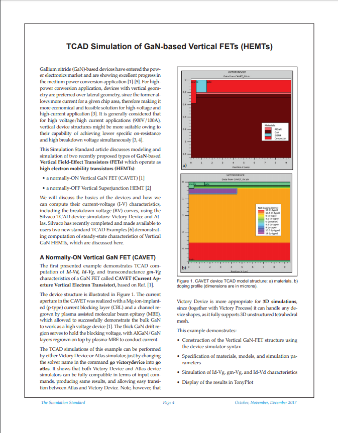
- a normally-ON Vertical GaN FET (CAVET) [1]
- a normally-OFF Vertical Superjunction HEMT [2]


