Stress Induced by Intrinsically Strained Silicon Nitride Passivation Films of AlGaN/GaN HEMTs Using Victory Process 2D
In the AlGaN/GaN HEMT fabrication process, silicon nitride (Si3N4) passivation of the HEMT surface layer, which is typically AlGaN, is commonly used to mitigate defect-related charge traps at the AlGaN surface. However, sufficiently thick Si3N4 passivation films manifest built-in or intrinsic stress that induces mechanical stress in underlying AlGaN/GaN HEMTs. Depending on deposition conditions, intrinsic stress in Si3N4 passivation films can be either compressive or tensile. Using Victory Process 2D to simulate stress induced by intrinsically strained passivation films of Si3N4 allows assessment of the influence such intrinsic stresses exerts on the AlGaN/ GaN HEMT performance.
Stress Simulation with Victory Process 2D
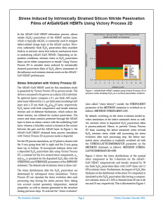
The AlGaN/GaN HEMT used for this simulation study is generated by Victory Process 2D in process mode. The device is assumed to be grown on a silicon (111) substrate. Its epitaxial layers comprise a 0.1 μm thick AlN nucleation layer followed by a 1 μm thick semi-insulating GaN layer and a 25 nm thick Al0.30Ga0.70N layer, respectively. Si3N3layers with both compressive and tensile intrinsic stresses and of different thicknesses, which induce different stresses, are utilized for surface passivation. The source and drain contacts penetrate through the AlGaN layer to form an ohmic contact with the underlying GaN layer, whereas a Schottky contact is formed at the contact between the gate and the AlGaN layer. In Figure 1, the AlGaN/GaN HEMT obtained from process simulation with Victory Process 2D in process mode is depicted.


