Simulating the Source of Polarization Charge in AlGaN/GaN HFETs
Polarization-induced charges at the AlGaN/GaN interface of heterojunction field-effect transistors (HFETs) create a high density, two-dimensional electron gas (2DEG) in the channel. One approach to simulating the 2DEG is to place a fixed positive charge at the AlGaN/GaN interface, thus attracting a fixed quantity of electrons to the channel. Silvaco’s ATLAS software can do this with either an INTERFACE statement or automatically with the use of the POLARIZATION parameter on the REGION statement. This is fine, as far as it goes, but this simple approach glosses over some nuances having to do with the source of carriers in the channel. A paper by Ibbetson, et al.,[1] explored this question theoretically and experimentally. Based on an analysis of the electrostatics of the structure, they determined that surface states at the top of the AlGaN barrier are the most likely source of the electrons attracted to the channel. This article demonstrates the simulation of this effect.
Ibbetson gave two possible explanations of the mechanism by which charge is transferred from the surface donor states to the 2DEG. Our simulations support his second explanation, that of surface pinning of the Fermi level. In wurtzite materials, the polarization has a spontaneous and a piezoelectric component. It is assumed that the relatively thick GaN buffer layer is unstrained, so it has only the spontaneous component. So fixed charges for GaN, 2.122e13 cm-2, are placed at the top (-2.122e13 cm-2) and bottom (+2.122e13 cm-2) of the buffer layer. The thin AlGaN layer is assumed to experience a uniform strain from its composition-dependent lattice mismatch with the GaN substrate. For the 34% AlN composition of AlGaN used in Ibbetson’s experiments, the nominal value of the total polarization charge is 4.005e13 cm-2, so -4.005e13 cm-2 is placed at the top surface of the AlGaN and +4.005e13 cm-2 is placed at the bottom, at the interface with GaN. Therefore, the total polarization charge placed at the interface is +1.883e13 cm-2, which would attract that density of electrons to the 2DEG in the channel. That is not exactly the density value actually found for the 2DEG. The density of the 2DEG varies with the thickness of the AlGaN layer.
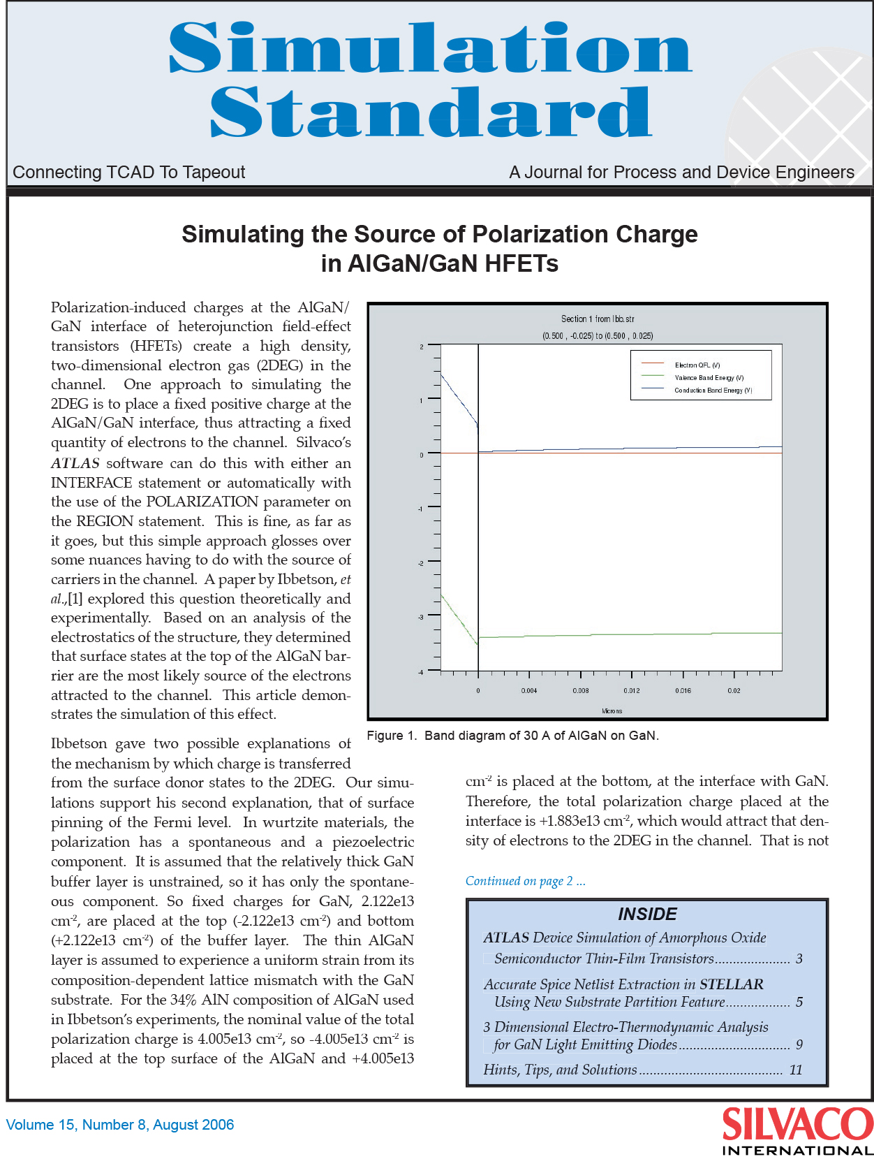
Figures 1 and 2 show that the Fermi level at the AlGaN surface is pinned at 2.6 volts above the valence band by the presence of the donor traps and the polarization charge. In Figure 1, the thickness of the AlGaN is 30 A. In this case, the Fermi level is below the GaN conduction band, so no accumulation of charges occurs in the channel.


