Compact Multi-Level Digital-to-Analog Conversion Using Thin-Film Multimodal Transistors
Unlike conventional ohmic contact thin-film transistors (TFTs), contact-controlled TFTs [1], [2] rely on source energy barriers to produce a range of benefits including: low saturation voltages; extremely high intrinsic gain; power-efficiency; electrical stability; and uniformity of operation, notably with imprecise processes [3]. Generally, these benefits come at the expense of transconductance, however in materials such as polysilicon, similar levels of on-current can be obtained in a more compact footprint without any trace of kink-effect [4], [5].
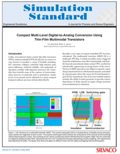
Recently, a new type of contact-controlled TFT has been introduced. The multimodal transistor (MMT) [2] is a multi-gate TFT (Fig. 1) which resembles many staggered electrode architectures, but offers functionality and benefits beyond conventional ohmic contact TFTs, enabled by intentionally engineering an energy barrier at the source. The key to MMT operation is its ability to separate source charge injection from on/off channel transport, controlled by separate gates above the source (CG1) and channel region (CG2), respectively. One of its most notable features includes the ability to tailor geometry to provide a linear dependence of drain current on input voltage (constant transconductance) in saturation.


