3D TFT Simulation of Grains and Grain Boundaries
Introduction
Low-temperature polycrystalline silicon (LTPS) thin-film transistors have been widely applied to AMOLED (Active Matrix Organic Light Emitting Diode) as the most suitable means for high mobility, high switching speed and high resolution [1-2].
A Laser Annealing Process such as Excimer Laser Annealing (ELA) is used to manufacture by converting Amorphous Silicon (a-Si) to Polycrystalline Silicon (poly-Si) at low temperature. The poly-Si structure (produced through ELA) shows the laser wavelength, pulse width and spatial beam dependencies.
Recently, the luminance non-uniformity induced by the threshold voltage deviations which arises from the non-uniform grain size and grain boundary has become known as one of the most important issues for OLED displays. Several approaches are proposed to perform 3D TFT simulation of grains and grain boundaries [3-4]. However, it is generally challenging due to the difficulties in generating realistic grain patterns.
This article discusses the newly implemented feature of Voronoi Grain Patterns in Victory Mesh to create realistic grains and grain boundaries. It also shows the results of different grain patterns as well as their influences with electrical characteristics.
1. Creation of Device Structures with Grains and Grain Boundaries Patterns
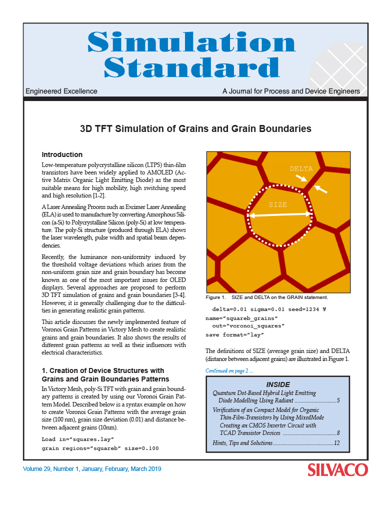
In Victory Mesh, poly-Si TFT with grain and grain boundary patterns is created by using our Voronoi Grain Pattern Model. Described below is a syntax example on how to create Voronoi Grain Patterns with the average grain size (100 nm), grain size deviation (0.01) and distance between adjacent grains (10nm).


