SURGE Virtual Event North America 2023

Silvaco held its annual SURGE users event on October 26, 2023. You may view the event in the archive below.

SURGE brings the TCAD, EDA, and IP communities together to discuss new technologies, share users’ experiences, and discover innovative techniques for advanced semiconductor design.

Agenda

GENERAL SESSION
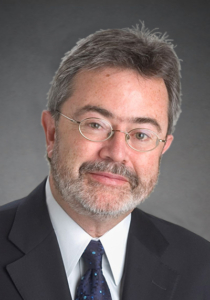
Welcome and Introduction - Dr. Babak Taheri – CEO and Board Member – Silvaco, Inc.​
Machine Learning: A New Revolution for EDA – Patrick Groeneveld, Ph.D.
TCAD Models as “Digital Twins" to Simulate and Optimize Semiconductor Manufacturing Processes – Raul Camposano, CTO, Silvaco, Inc.

TCAD TRACK
TCAD Simulation Update – Dr. Eric Guichard, SVP and GM of TCAD Business Unit, Silvaco​, Inc.
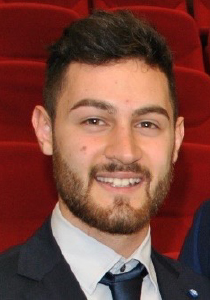
Impact of Surface Defect Dot on Short Circuit Phenomena – Salvatore Cascino,  SiC R&D Engineer, STMicroelectronics​
Study of Magnesium Activation Effect on Pinch-Off Voltage of Normally-Off p-GaN HEMTs for Power Applications – Giovanni Giorgino, GaN Device Engineer for ADG R&D Power & Discretes, STMicroelectronics​
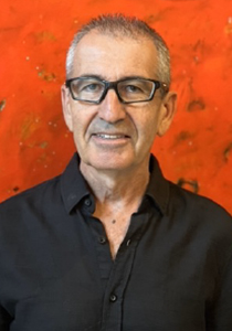
Silvaco Simulation Tools Assisting GaN-based Power Devices Design and Development – Dr. Eldad Bahat-Treidel, Senior Scientist, Ferdinand-Braun-Institut
Going Beyond CMOS in Memories – Debo Olaosebikan Ph.D., Co-Founder and CEO, Kepler Computing ​
Transport at the Nanoscale for CMOS and RRAM Applications – François Triozon, Research Scientist, CEA-Leti
Numerical Simulations of Spintronic Magnetoresistive Memories – Nils Jørstad, PhD Researcher, TU Wien
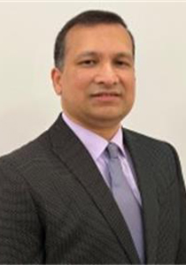
Advanced Modeling Solutions for Development and Manufacturing of Memory Technologies – Sumeet Pandey, Distinguished Member of Technical Staff, Micron​ Technology
25 Years of Quantum Transport Tool Development Resulting in a Global Impact – Gerhard Klimeck, Deputy CIO, Associate VP of Academic Research, Purdue University​
Simulation of 2D-TMDs-channel FETs with Atomistic Precision – Dr. Phillipe Blaise, Silvaco, Inc.​

EDA AND IP TRACK
Analog Custom Design and IP Update – Dan Fitzpatrick, VP and GM of EDA Business Unit, Silvaco, Inc.​
Power Device Modeling for SPICE – Bogdan Tudor, Silvaco, Inc.
Silvaco and Tower Collaboration in Design Kit and Standard Cell Library Development and QA – Ofer Tamir, Managing Director, CAD, Design Enablement and Support, Tower Semiconductor
A High Speed, Reliable, Low Voltage SRAM for Efficient Compute – Sinan Doluca, VP of Technology, Aril, Inc.​
Designing High-Performance I/O for Cryogenic Applications with Silvaco Analog Custom Design Platform – Ahmad S. Mazumder / Shaikh Shams, Silvaco, Inc.​
Advanced Parasitics Analysis Demonstration with Viso - Ayoub HAGROU, Analog Design Engineer, STMicroelectronics

Speaker:

Dr. Babak Taheri, Chief Executive Officer and Board Member
Silvaco, Inc.

Babak A. Taheri, Ph.D., has served as Silvaco’s Chief Executive Officer and member of Silvaco’s board of directors from August 2019 to September 2021 and from November 2021 to present. From October 2018 to August 2019, Dr. Taheri served as Silvaco’s Chief Technology Officer and Executive Vice President of Products. Prior to joining Silvaco, Dr. Taheri served as Chief Executive Officer and President of Integrated Biosensing Technologies (IBT), an advisory and consulting firm, from May 2015 to October 2018. Dr. Taheri has also served on various advisory boards, including MEMS World Summit, a conference for MEMS manufacturers, equipment and material suppliers and research institutes, Novasentis, Inc., an electromechanical polymer technology development company, and as the advisory board chair of the electrical engineering department at the University of California, Davis. Dr. Taheri also served on the board of directors of Parisi House on The Hill, a residential alcohol and drug non-profit, from June 2021 to May 2022. Dr. Taheri received a B.S. in engineering from San Francisco State University, a M.S. in electrical engineering from San Jose State University and a Ph.D. in biomedical engineering from the University of California, Davis.

Patrick Groeneveld

Machine Learning: A New Revolution for EDA

Abstract:

The EDA design flow uses a complex chain of algorithms to transform a functional description into a mask pattern. Some of the algorithms use numerical solvers, others are just clever heuristics that have proven to work. Each algorithm has a large variety of parameters that are hand-tuned tuned for best results. For instance, area and speed are traded off using relative cost parameters. Some recent tools apply Machine learning to automatically converge quickly on a design-specific set of parameters. This is done by brute force running the flow many times and using PPA data to discover the gradients.

Research work is done on making true ML-driven EDA tools. Some address placement, other routing strategies. In this presentation we will address the state of the art of ML in EDA flows and present an outlook of its impact in the coming decade.

Speaker:

Dr. Patrick Groeneveld

Dr. Patrick Groenveld. Patrick has worked at Magma, Cadence, Synopsys and Cerebras, and he lectures at Stanford. He has worked for many years in the EDA industry. He was Chief Technologist at Magma Design Automation where he was part of the team that developed a groundbreaking RTL-to-GDS2 synthesis product. Patrick was also a Full Professor of Electrical Engineering at Eindhoven University. He is a lecturer in the EE department at Stanford University and serves as finance chair in the Executive Committee of the Design Automation Conference. Patrick received his MSc and PhD degrees from Delft University of Technology in the Netherlands.

Ofer Tamir

Silvaco and Tower Collaboration in Design Kit and Standard Cell Library Development and QA

Abstract:

Silvaco is the main Standard Cell library provider for Tower cross all technologies. Recently we developed libraries for 65nm advanced Power Management process that includes advance characterization and MTBF performance calculation.

Silvaco has a full analog design flow and Tower as the lead analog foundry to support and qualify its iPDK and SPICE using Silvaco’s flow – including tools like – Expert , Gateway , SmartLVS and SmartDRC.

Speaker:

Ofer Tamir, Managing Director, CAD, Design Enablement and Support
Tower Semiconductor

Ofer joined Tower in 2001 as Director of Design enablement and CAD. Ofer is responsible for all design kits development, WW design support and CAD teams. Has more than 30 years of EDA and CAD experience, working at National Semiconductor (Now TI), DSPG and Tower. Ofer is also responsible for EDA relations and as such participates and presents at different technical conferences – such as DAC, Tech forums, and more.

Eric Guichard

TCAD Simulation Update

Abstract:

Dr. Guichard will provide an update on Silvaco TCAD Victory simulation products, the importance of TCAD in the development of next-generation devices, and the future of TCAD development.

Speaker:

Dr Eric Guichard, SVP and GM of TCAD Business Unit
Silvaco, Inc.

Eric Guichard, Ph.D., has served as Silvaco’s Senior Vice President and General Manager of TCAD Business Unit since November 2012, and as Silvaco’s Vice President of Applications from July 2008 to November 2012. From September 1995 to July 2008, Dr. Guichard served in various roles with Silvaco SA, formerly known as Silvaco Data Systems, one of Silvaco’s wholly-owned subsidiaries, including as an applications engineer. Dr. Guichard received a M.S. in material science and a Ph.D. in semiconductor physics from Institut Polytechnique de Grenoble, France.

Salvatore CASCINO

Impact of Surface Defect Dot on Short Circuit Phenomena

Abstract:

During switching operations, it can happen devices could be reaching overload abnormal condition. Some applications require robustness specifications (for example in Short Circuit and UIS test). Such phenomena can be simulated by mixed-mode circuits and an accurate tuning of simulation parameters, thanks to simulation/experiment information exchange, allows us to predict electrothermal behavior during dynamic phase. As an example, we report here a study of short circuit phenomenon. Impact on short circuit of a defect localized in active area has been investigated by means of TCAD simulations performed with Silvaco software. Different cases have been studied in which the defect dot was localized at flat interface body/drain, at SiC/oxide interface in the channel region, at curved interface body/drain. A sensitivity with position has been performed too.

Speaker:

Salvatore Cascino, SiC R&D Engineer
ST Microelectronics

Salvatore Cascino was born in Palermo (Italy) in 1970. He obtained a Degree in Physics from the University of Palermo. He was involved at ENEA (Frascati – Rome) with Nuclear Fusion Department (FTU project) and with the Fusion Research group in Padua (RFX project). He is currently at STMicroelectronics (Catania) with the R&D Group and his current research interest is aimed to technology development for Silicon Carbide devices. In the past he worked on development of devices for sensing applications and radiofrequency, too.

Giovanni Giorgino

Study of Magnesium Activation Effect on Pinch-Off Voltage of Normally-Off p-GaN HEMTs for Power Applications

Abstract:

The role of the magnesium (Mg) doping and its electrical activation on the off-state of p-GaN/AlGaN/GaN HEMTs has been investigated in this work. Firstly, the effect of different Mg doping profiles has been studied via the help of Technology Computer-Aided Design (TCAD) simulations, with the objective of analyzing the band diagrams of the structure. Then, it has been shown how experimental Capacitance–Voltage measurements can be useful to obtain information on the net acceptor concentration in the p-GaN.

As a result, devices with an undoped (magnesium-free) GaN gate have been experimentally compared to devices whose p-GaN gate has been activated via a reference annealing process. Finally, results on a device characterized by an improved p-GaN activation have been presented and compared, showing improvements on several parameters of both off- and on-state, thus underlining the key role of the Mg activation process in the overall performances of normally-off GaN HEMTs.

Speaker:

Giovanni Giorgino, GaN Device Engineer for ADG R&D Power & Discretes
STMicroelectronics

Giovanni Giorgino received his master’s degree in electronic engineering from Polytechnic University of Turin, Italy, in 2020. Since 2020 he is working as GaN Device Engineer at STMicroelectronics of Catania in R&D department. He has a background in semiconductor physics, analog and power electronics. He is currently involved in the development, characterization and modelling of p-GaN gate devices for power applications.

Power Device Modeling for SPICE

Abstract:

We start by examining the different technologies used in the manufacturing of power devices, including Si, GaN and SiC, considering their respective particularities and advantages.

We will then analyze various approaches to the SPICE modeling of Power devices, including compact models and macromodels.

A significant portion of our presentation will be dedicated to the topic of Power FET modeling. In particular we will illustrate how to properly address their specific bias-dependent capacitances and how to deal with model tuning based on dynamic characteristics.

Finally, we will share some of our expertise in dealing with the unique challenges of power devices, including parasitic elements and model accuracy.

Speaker:

Bogdan Tudor, Senior Manager, Device Characterization
Silvaco, Inc.​

Bogdan Tudor is Head of Device Characterization for Silvaco, leading the Utmost and Modeling Service teams. He has over 20 years of experience in model development and characterization software.

​​​

Silvaco Simulation Tools Assisting GaN-based Power Devices Design and Development

Abstract

Large amount of research efforts was invested in the last two decades in wideband gap GaN based lateral power devices, which are currently approaching commercial maturity for power electronic switching up to 650 V class. Yet, they do not approach their theoretical material limit, in terms of RDS_ON × A vs. VBr. Among the reasons for this limitation are trade off between the blocking strength and the increase of dispersion and the vertical blocking strength of GaN on Si substrates. Among the different approaches to overcome these challenges, two device technologies may be pointed out; vertical GaN based devices and ultra-wideband gap lateral HFET with AlN buffer. Vertical GaN based transistors are desired due to their reduced wafer “foot print”, in comparison to lateral HFETs, that results in a reduction of RDS_ON × A by one order of magnitude down to 1.0 m∙cm2. In addition, the possibility of strain free homoepitaxy allows the growth of thick drift layers with low residual background doping for blocking capability larger than 1 kV. Lateral GaN based transistors (HFETs) with un-intentional doped AlN as buffer material and with high conduction band offset at the AlN-buffer / GaN channel interface should effectively confine the GaN transistor channel. This will result into blocking strength enhancement and low dispersion effects.

Physical based simulation tools are essential for the development and insight to these new generation of wide band gap electronic devices in FBH laboratories. In this talk, we will give examples for the use of “Silvaco” simulation tools used to design, predict and analysis the electrical characterization of vertical and lateral GaN based power devices. The conductance properties of GaN based fin MISFETs are explored and compared to experimental characteristics. The conductance properties are predicted with the variation of geometrical dimensions and the epitaxial layers properties. Edge termination topologies in vertical GaN devices are engineered using avalanche models and compared to experimental and theoretical values. Finally, insight to trapping and de trapping effects AlN / GaN lateral HFET gives explanation to dynamic ON state resistance peculiarity using avalanche model specific to the device epitaxial structure.

Speaker:

Dr. Eldad Bahat-Treidel, Senior Scientist
Ferdinand-Braun-Institut (FBH)

Eldad Bahat-Treidel received his B.Sc. degree in chemical process engineering and M.Sc. degree in electro-optic engineering from Ben Gurion University, Be’er Sheva, Israel in 1996 and 2004 respectively. He received his Ph.D. ( Dr. Ing. ) in electrical engineering from the Technische Universität Berlin Germany in 2012. In 1996 he joint Intel electronics LTD as a photolithography critical layers process engineer, and then joined in 2004 Tower semiconductor LTD as a senior research and development photolithography engineer. In 2006 he joined the Ferdinand-Braun-Institut gGmbH, Leibniz-Institut für Höchstfrequenztechnik (FBH) in Berlin for the development GaN switching transistors for high voltage power electronics applications. Since 2014 he is working on the research and development of innovative electronic devices such vertical GaN based transistors.

Debp

Going Beyond CMOS in Memories

Abstract:

In his presentation to Silvaco’s User Group, Debo will introduce Kepler Computing, talk on why Kepler was formed, what the company is doing to enable Design Beyond CMOS, particularly for memory applications, and the use of Silvaco TCAD to simulate these new memories.

Speaker:

Debo Olaosebikan, Co-Founder and CEO
Kepler Computing

Debo is an entrepreneur, physicist and engineer based in San Francisco who, prior to Kepler, was Co-Founder and Chief Technology Officer of Gigster. He was a physics PhD candidate at Cornell University, where he was lead researcher from Cornell working to build an electric silicon laser. He researched spintronics at IBM Almaden and was the Future Africa Awards – Best Use of Science Winner in 2011. Debo invests and advises startups and was a mentor at the Thiel Fellowship.

François Triozon

Transport at the Nanoscale for CMOS and RRAM Applications

Abstract:

Accurate simulation of electron transport at the nanoscale becomes crucial for advanced CMOS devices and RRAM technologies. In this talk, we review recent progress in quantum transport simulation and their benefits for device optimization. 3D simulations based on the Non-Equilibrium Green’s Functions (NEGF) formalism allow accurate evaluation of access resistances in tri-gate CMOS devices. Similar methods are currently used to evaluate contact resistances in transistors with channels made of 2D materials. We will also discuss some simulation challenges for RRAM devices (OxRAM, tunnel junctions), since the coupling between ab initio simulations and quantum transport does not yet provide a complete picture of device operation.

Speaker:

François Triozon, Research Scientist
CEA-Leti, Grenoble, France

François TRIOZON received the Ph.D. degree from University Grenoble Alpes, France, in 2002. Since 2005 he is a permanent researcher at CEA-Leti, Grenoble, France. His main research interest is the simulation of electron transport in nanodevices, using both semi-classical and quantum methods, from atomic scale (ab initio) to full device simulations. His research covers various devices and materials: carbon nanotubes, 2D materials, CMOS silicon devices, GaN power devices, ferroelectrics, and OxRAMs.

Nils Petter Jørstad

Numerical Simulations of Spintronic Magnetoresistive Memories

Abstract:

Magnetoresistive random access memory (MRAM) is a promising candidate for replacing the current charge-based memory technologies due to its high speed, endurance, and nonvolatility. Several approaches have been proposed for efficient manipulation of the logical state by taking advantage of spin-polarized currents. The demand for flexible simulation software capable of simulating the operation of MRAM is high, as several engineering challenges limit the wide adoption of MRAM. We present recent progress and results from the development of a finite element method approach to simulating the charge, spin, and magnetization dynamics in MRAM cells.

Speaker:

Nils Petter Jørstad
Christian Doppler Laboratory for Nonvolatile Magnetoresisitve Memory and Logic (CDL-NovoMemLog), Institute of Microelectronics, TU Wien

Nils Petter Jørstad was born in Warsaw, Poland, in 1995. He received his Master’s degree in Physics at the Norwegian University of Science and Technology (NTNU), Norway, in 2021, specializing in computational physics. Nils joined the Christian Doppler Laboratory for Nonvolatile Magnetoresistive Memory and Logic at the Institute for Microelectronics, TU Wien, in 2021, where he is pursuing a PhD degree focusing on the implementation of spin and magnetization dynamics in simulations of nonvolatile magnetoresistive memory devices.

Digital Twins for Semiconductor Manufacturing

Abstract:

TCAD models are used to simulate the fabrication and operation of semiconductor devices. TCAD has become essential in the deployment of new semiconductor technology. With increasing accuracy, TCAD models can now be used as “digital twins” to simulate and optimize semiconductor manufacturing processes.

This opens up many new applications, such as virtual development of new semiconductor technology, reducing the need for physical experimentation, and ultimately shortening development time and time to yield. Digital twins can also be used during production in the fab to further optimize processes, monitor variations, and detect malfunctions. This presentation will delve into these concepts and provide examples of TCAD that can be used as digital twins.

Speaker:

Raúl Camposano, Ph.D, Chief Technology Officer
Silvaco, Inc.​

Raúl Camposano, Ph.D., has served as Silvaco’s Chief Technology Officer since February 2022. Dr. Camposano has served as a partner at Silicon Catalyst LLC, an incubator for semiconductor solutions, since April 2015 and as a lecturer on EDA and Machine Learning Hardware at Stanford since April 2018. From July 2020 to January 2022, Dr. Camposano served as an advisor to Applied Materials, Inc., a semiconductor equipment company. From August 2015 to July 2020, Dr. Camposano served as Chief Executive Officer of Sage Design Automation, Ltd., a software tools company acquired by Applied Materials in 2020. From November 2010 to May 2014, Dr. Camposano served as Chief Executive Officer of Nimbic, Inc., an EDA cloud company, acquired by Mentor Graphics Corporation in 2014. From January 1994 to January 2007, Dr. Camposano served in various roles at Synopsys, an EDA solutions company, including as its Chief Technology Officer, Senior Vice President, and General Manager. Prior to that, Dr. Camposano served on the board of directors of the German National Research Center for Computer Science, as a professor of computer science at the University of Paderborn, and as a Research Staff Member at the IBM T.J. Watson Research Center. Dr. Camposano received a B.S. and M.S. in electrical engineering from Universidad de Chile and a Ph.D. in computer science from Karlsruhe Institute of Technology. Dr. Camposano was elected as a Fellow of the IEEE in 1999 and to serve on the board of directors of ESDA, the EDA Consortium, in 2012.

Advanced Modeling Solutions for Development and Manufacturing of Memory Technologies

text

Gerhard Klimeck

25 Years of Quantum Transport Tool Development Resulting in a Global Impact

Abstract:

The quantum transport modeling community has debated the virtues of various theoretical approaches and prototype implementations over the past 30 years. Early 1980/90s prototypical devices were based on 2-D electron gases (2DEGs) or room-temperature resonant tunneling diodes. We have come full term and find the critical size and operational characteristics of these early devices in today’s nano-scaled transistors. Today industry requires quantitative, predictive device design models to explore the design paths towards devices at the ultimate few nanometer scaling limit. This presentation will describe the critical reasons why industry has adopted the Non-Equilibrium Green Function (NEGF) methodology with an atomistic tight-binding basis. Our NEMO5 implementation defined the state-of-the-art that is now adopted by the community, is used today at Intel and commercialized by Silvaco. nanoHUB and chipshub disseminate various NEMO versions through simple-to-use apps such that students and researchers can explore concepts and performed detailed analysis.

Speaker:

Gerhard Klimeck, Professor and nanoHUB Director
Purdue University

Dr. Gerhard Klimeck is a Chaired Professor of Electrical and Computer Engineering at Purdue University; Deputy CIO and Associate Vice President for Academic IT; Director of the Network for Computational Nanotechnology; Reilly Director of the Center for Predictive Materials and Devices. He helped to create nanoHUB.org, the largest virtual nanotechnology user facility serving over 2.0 million global users, annually. Dr. Klimeck is a fellow of the Institute of Physics (IOP), the American Physical Society (APS), the Institute of Electrical and Electronics Engineers (IEEE), the American Association for the Advancement of Science (AAAS), and the German Humboldt Foundation. He has published over 525 printed scientific articles; he has been recognized for his co-invention of a single-atom transistor, quantum mechanical modeling theory, and simulation tools. His NEMO5 software has been used since 2015 at Intel to design nano-scaled design transistors. The nanoHUB team was recently recognized by a top 100 by R&D award – Making simulation and data pervasive.

Philippe Blaise

Simulation of 2D-TMDs-channel FETs with Atomistic Precision

Abstract:

Are the 2D-channel transistors suitable candidates for the replacement of Si? Taking into account the extreme scaling down to a few atomic layers of the FET channel, only an atomistic solution looks viable. In this context, we show how the Victory Atomistic tool can answer this essential question thanks to quantum mechanics, offering valuable support for the prototyping effort of a 2D transistor in a professional TCAD environment.

Speaker:

Dr. Philippe Blaise, Senior Application Engineer
Silvaco, Inc.

Dr. Philippe Blaise has been a senior application engineer in atomistic simulation at Silvaco’s TCAD Division for three years. Prior to joining Silvaco, Dr. Blaise was a senior engineer specialized in atomistic simulation of new memory devices and transistors at CEA/LETI for 15 years. He is a former member of the IEEE IEDM Modelling and Simulation Committee. He is co-author of more than 50 papers in peer-review journals in the field and 30 contributions to conferences and workshops, plus 5 patents and one book chapter.

Dr. Blaise holds a Master’s degree in applied mathematics from ENSIMAG engineering school and a Ph.D. in solid states physics from the Université Grenoble Alpes, France.

Analog Custom Design Update

Abstract:

Dan FitzPatrick will provide an update on Silvaco’s Analog Custom Design product portfolio, new features and functionality, and the future of Silvaco’s EDA solutions.

Speaker:

Dan Fitzpatrick, VP and GM of EDA Business Unit
Silvaco, Inc​​​

Dan FitzPatrick is Vice President and General Manager of the EDA Business Unit. He is responsible for managing the development of all EDA tools including analog custom design and verification, circuit simulation and SPICE modeling, standard cell layout generation and characterization and SIP management tools. Dan joined Silvaco in 2021, leading SIP management, standard cell layout generation and characterization product lines. Dan has an extensive EDA background and many years of experience in software development and product management from startups to fortune 500 companies. Dan holds a MSEE from the University of Florida and an MBA from the University of Central Florida.

High Speed, Reliable, Low Voltage SRAM for Efficient Compute

Abstract:

Efficiency is critical for next generation systems whether they are battery operated devices or AI/ML accelerators in the cloud infrastructure. Operating the logic and SRAM technology at the same voltage and leveraging dynamic voltage and frequency scaling can deliver maximum performance and efficiency but is often limited by voltage capability, speed and reliability of the SRAM macros.

A new SRAM technology, optimized on state-of-the-art CMOS technology, targets high speed, robust/reliable operation over a wide voltage range from 0.45V to 0.8V and above. The high speed, low voltage SRAM technology can be combined with efficient microarchitecture and optimized physical design to maximize performance per watt for compute, graphics, or AI/ML engines.

Speaker:

Sinan Doluca
VP of Technology, Aril, Inc.

Designing High Performance I/O for Cryogenic Applications

Abstract:

The Silvaco Analog and Interface IP team recently designed and delivered a very high speed 2Gbs fully functional LVDS I/O operating at 4K (-269C). The Silvaco modeling team created model files at this extreme temperature and the IP team designed, laid out and created collaterals/views with Silvaco EDA tools. The devices’ characteristics do not follow regular characteristics seen at standard temperatures (-55C to 125C) and making it functional at 4K is by no means an easy challenge.

The LVDS PHY included transmitter, receiver and an accessory block satisfying PVT independent performance which included 3.5mA current drive by the transmitter @100-ohm load and PVT independent 100 ohm terminated between the PAD+ and PAD- terminals of the Receiver. Furthermore, the Transistor also included programmable equalization to provide board, SI (Signal Integrity) and PI (Power Integrity) compliant performance.

Speakers:

Ahmad S. Mazumder, Director of Engineering
Silvaco, Inc.

Ahmad S Mazumder is a Director of Engineering in the IP Division of Silvaco. He is responsible for Development & Customer support in all Analog and Interface IPs. He is an Industry veteran on the development of High-Speed Memory & Interface IPs and all sorts of analog IPs. He worked on cutting edge DDR, extreme High-speed SerDes, Interfaces, ESD, Quality & Reliability for 28 years at various SOC companies – Intel, Broadcom, C-Cube Microsystems etc. He joined Silvaco’s IP Engineering Division in 2019 and is Instrumental in growing Analog/IP business at an accelerated rate.
Ahmad S Mazumder holds an MS in VLSI Semiconductor Design from the City University of New York and BS in Electrical & Electronics Engineering from Bangladesh University of Engineering and Technology.

Shaikh A Shams, Staff Engineer
Silvaco, Inc.

Shaikh A Shams is a Staff Engineer in the Analog/Interface IP Division of Silvaco. He is responsible for developing Analog and Interface IPs at Silvaco. He worked on High-speed SerDes, Interfaces, Voltage Regulators, AMS Design and Verification for 22 years at different companies – Intel Corporation, Global Foundries and Dialog Semiconductor. He joined Silvaco’s IP Engineering Division in 2020. Shaikh A Shams holds an MS in Electrical and Computer Engineering from the University of Arizona.

Ayoub HAGROU

Advanced Parasitics Analysis Demonstration with Viso

Abstract:

Viso is a next generation parasitics analysis solution that quickly analyzes the electrical properties of RC parasitic networks, which can crucially impact circuit behavior. Viso’s parasitics-focused approach enables fast analysis of interconnects to pinpoint problem areas. Viso provides a highly intuitive user interface to highlight problematic parasitics, timing estimation and accurate comparison of different extracted netlists.

In this session we will demonstrate the power and capabilities of Viso in a real-world circuit design.

Speaker:

Ayoub Hagrou, Analog Design Engineer
STMicroelectronics

Ayoub Hagrou works as Analog Design Engineer for STM32 General Purpose Microcontroller Products in the MDG division of STMicroelectronics.