Automated Stress Simulation Interface Between Victory Process and Device
1.0 Introduction
Victory Process now includes the Victory Stress library directly within the process simulator, which removes the necessity to keep switching from process to stress simulators when invoking stress simulations at many steps during process simulation. For standard silicon type processes, the main objective for including stress simulations during process simulation, is to include stress effects in the device simulation. A desirable feature, therefore, is for the stress and strain fields calculated during process simulation, to be carried over automatically into the device simulator. This feature has now been included in Victory Device, and is the subject of this article.
2.0 The P-Channel 7nm Tri-FinFET Test Structure
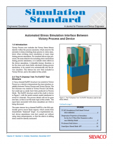
A 7nm p-channel FinFET structure was created in Victory Process as a vehicle to demonstrate the stress interface capability between Victory Process and Victory Device. The test structure was created in Victory Process Cell Mode, but could just as easily have been produced in Process Mode. The FinFET structure used in this study is shown in Figure 1, with the metal contacts made translucent to reveal it’s internals. The process details will not be gone into here, as that is not the main topic of this article. The input lines associated with stress simulation are what is being discussed.
The main stressor for p-channel FinFETs is the SiGe epitaxially grown source-drain regions, which creates their characteristic “diamond” shape. As a experimental control, device simulations were first carried out without using stress enhancements, so that the effects of adding stress could be directly measured.


