Simulation Standard
Technical Journal
A Journal for Process and Device Engineers
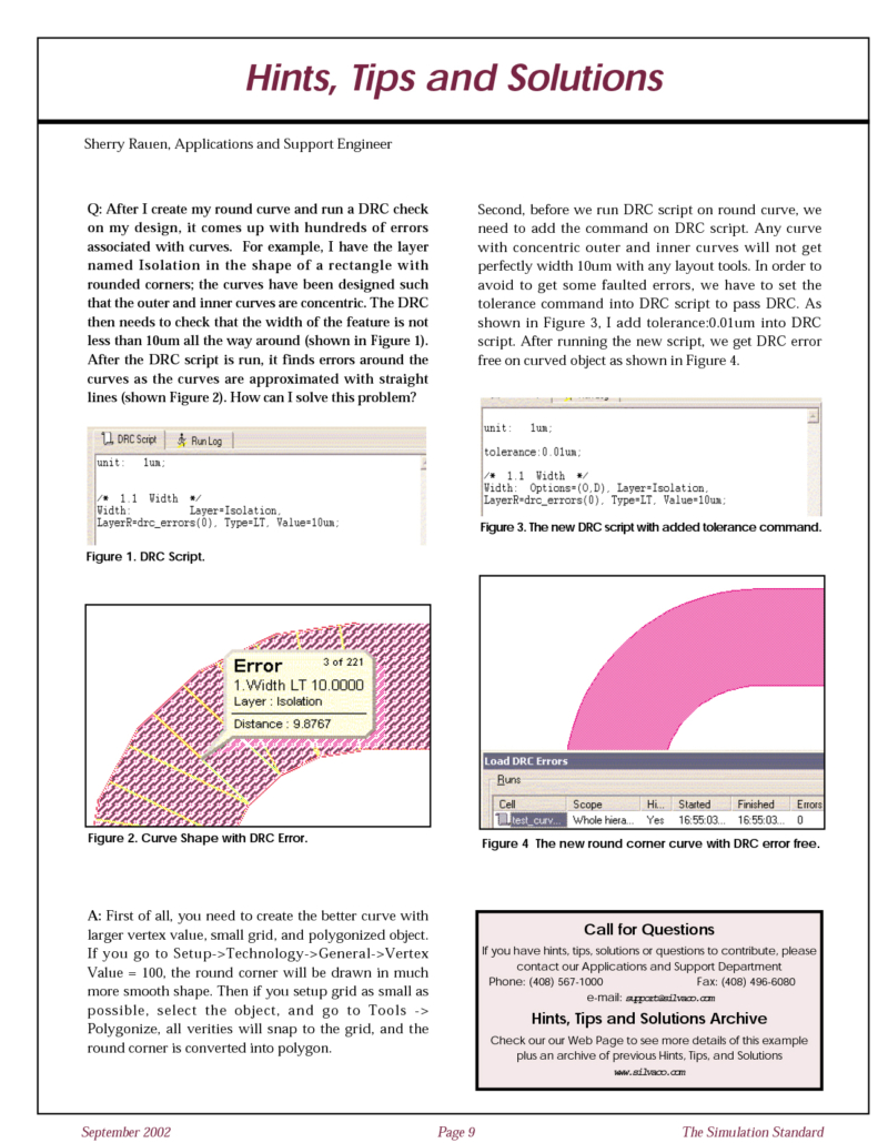
Running a DRC Check on a Design with Round Curves
After I create my round curve and run a DRC check on my design, it comes up with hundreds of errors associated with curves. For example, I have the layer named Isolation in the shape of a rectangle with rounded corners; the curves have been designed such that the outer and inner curves are concentric. The DRC then needs to check that the width of the feature is not less than 10um all the way around (shown in Figure 1). After the DRC script is run, it finds errors around the curves as the curves are approximated with straight lines (shown Figure 2). How can I solve this problem?
Simulating Boron Diffusion in Silicon Germanium
The silicon germanium heterojunction bipolar transistor (SiGe HBT) is a promising technology for combining the operating speed of compound material devices with the production capability of bulk silicon. The presence of a narrower-bandgap material in the base region where most of the bandgap offset occurs in the valence band, creates an energy well for holes. With the lower energy barrier, a lower hole current density can be obtained for a given electron current density increasing the transistor’s gain [1]. Thus the base can then be highly doped, greatly increasing high frequency performance whilst still retaining a reasonable gain. For this reason, the diffusion of boron in SiGe is of great interest.
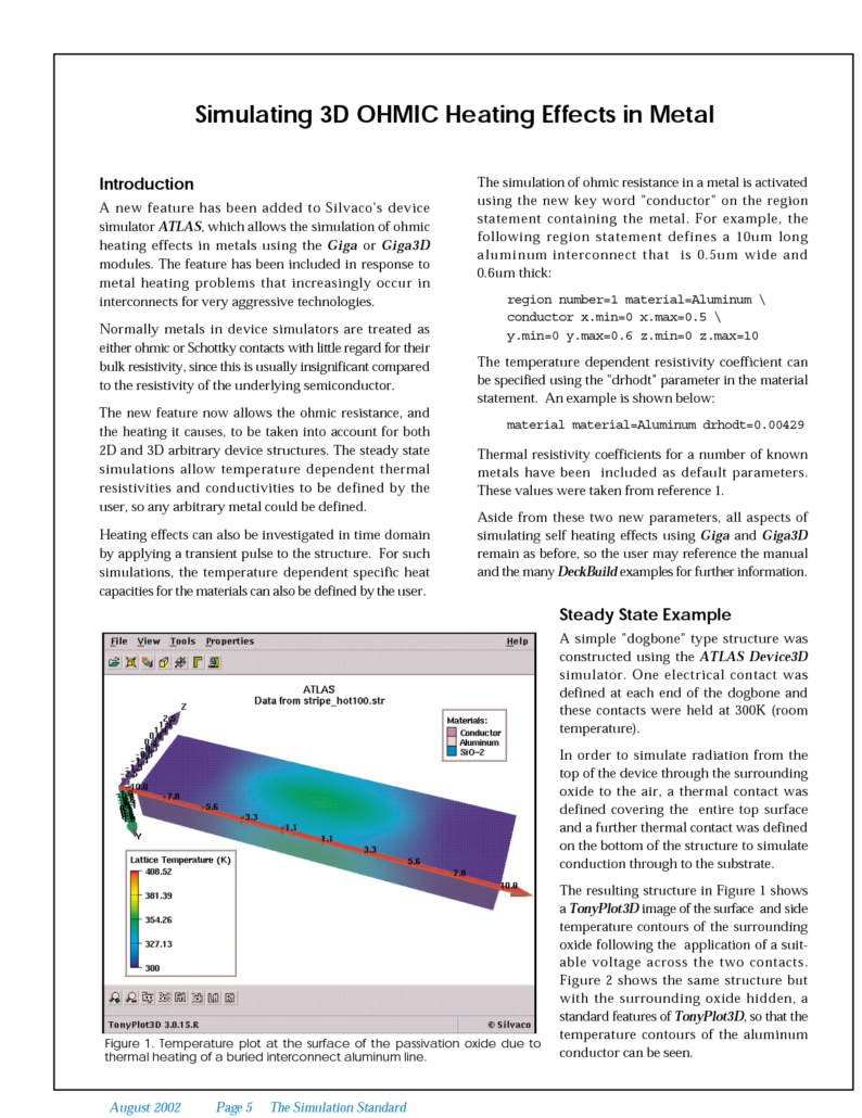
Simulating 3D Ohmic Heating Effects in Metal
A new feature has been added to Silvaco's device simulator ATLAS, which allows the simulation of ohmic heating effects in metals using the Giga or Giga3D modules. The feature has been included in response to metal heating problems that increasingly occur in interconnects for very aggressive technologies.
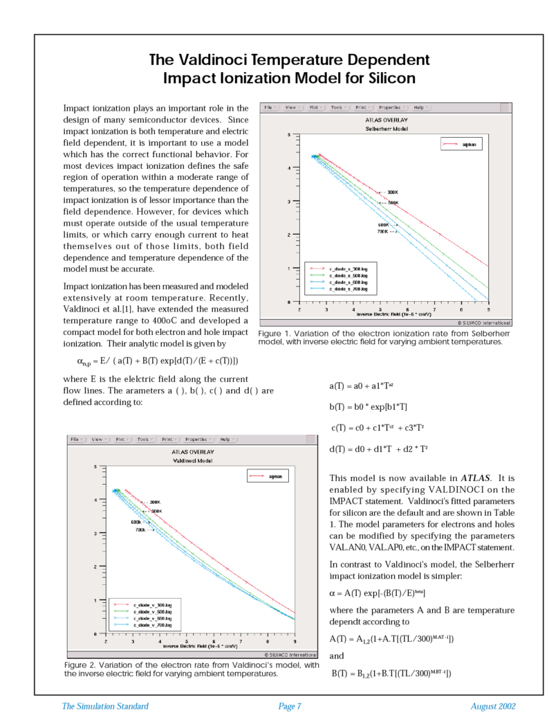
The Valdinoci Temperature Dependent Impact Ionization Model for Silicon
Impact ionization plays an important role in the design of many semiconductor devices. Since impact ionization is both temperature and electric field dependent, it is important to use a model which has the correct functional behavior. For most devices impact ionization defines the safe region of operation within a moderate range of temperatures, so the temperature dependence of impact ionization is of lessor importance than the field dependence. However, for devices which must operate outside of the usual temperature limits, or which carry enough current to heat themselves out of those limits, both field dependence and temperature dependence of the model must be accurate.
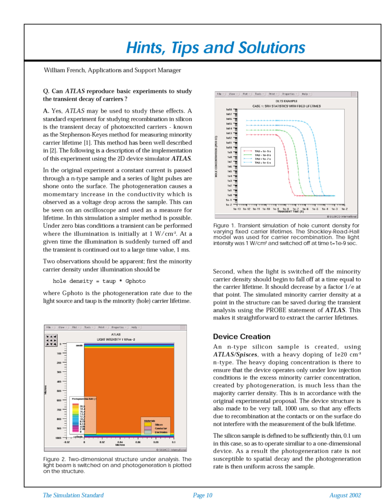
Reproducing Basic Experiments in ATLAS to Study the Transient Decay of Carriers
ATLAS may be used to study these effects. A standard experiment for studying recombination in silicon is the transient decay of photoexcited carriers - known as the Stephenson-Keyes method for measuring minority carrier lifetime [1]. This method has been well described in [2]. The following is a description of the implementation of this experiment using the 2D device simulator ATLAS.
BSIM3SOI Version 3.0 Model Released in SmartSpice
BSIM3SOI version 3.0 model was released on May 2002 by UC Berkeley. This model includes both Partially and Fully depleted models. This model is now implemented in SmartSpice and can be selected according to LEVEL selector.

