 https://silvaco.com/wp-content/uploads/2020/03/simstd_Q1_2009_a2.jpg
1012
782
Ingrid Schwarz
/wp-content/uploads/2019/11/silvaco-logo.png
Ingrid Schwarz2009-01-01 14:46:592021-07-16 21:46:16Self-Heating effect Simulation of GaN HFET Devices – 4H-SiC and Sapphire Substrate Comparison
https://silvaco.com/wp-content/uploads/2020/03/simstd_Q1_2009_a2.jpg
1012
782
Ingrid Schwarz
/wp-content/uploads/2019/11/silvaco-logo.png
Ingrid Schwarz2009-01-01 14:46:592021-07-16 21:46:16Self-Heating effect Simulation of GaN HFET Devices – 4H-SiC and Sapphire Substrate Comparison https://silvaco.com/wp-content/uploads/2020/03/simstd_Q1_2009_a1.jpg
1012
782
Ingrid Schwarz
/wp-content/uploads/2019/11/silvaco-logo.png
Ingrid Schwarz2009-01-01 14:41:542021-07-16 21:46:16Modeling of GaInP/GaAs DualJunction Solar Cells Including Tunnel Junction
https://silvaco.com/wp-content/uploads/2020/03/simstd_Q1_2009_a1.jpg
1012
782
Ingrid Schwarz
/wp-content/uploads/2019/11/silvaco-logo.png
Ingrid Schwarz2009-01-01 14:41:542021-07-16 21:46:16Modeling of GaInP/GaAs DualJunction Solar Cells Including Tunnel Junction https://silvaco.com/wp-content/uploads/simulationstandard/simstd_nov_2007_a2.jpg
1669
1344
Erick Castellon
/wp-content/uploads/2019/11/silvaco-logo.png
Erick Castellon2007-11-01 00:02:092021-07-16 21:46:30Ballistic Quantum Transport in Nanoscale Transistors: a Non Equilibrium Green’s Function Approach
https://silvaco.com/wp-content/uploads/simulationstandard/simstd_nov_2007_a2.jpg
1669
1344
Erick Castellon
/wp-content/uploads/2019/11/silvaco-logo.png
Erick Castellon2007-11-01 00:02:092021-07-16 21:46:30Ballistic Quantum Transport in Nanoscale Transistors: a Non Equilibrium Green’s Function Approach https://silvaco.com/wp-content/uploads/simulationstandard/simstd_nov_2007_a1-e1611191624800.jpg
1000
750
Erick Castellon
/wp-content/uploads/2019/11/silvaco-logo.png
Erick Castellon2007-11-01 00:01:492021-07-16 21:46:31A Novel Approach to Three-Dimensional Semiconductor Process Simulation: Application to Thermal Oxidation
https://silvaco.com/wp-content/uploads/simulationstandard/simstd_nov_2007_a1-e1611191624800.jpg
1000
750
Erick Castellon
/wp-content/uploads/2019/11/silvaco-logo.png
Erick Castellon2007-11-01 00:01:492021-07-16 21:46:31A Novel Approach to Three-Dimensional Semiconductor Process Simulation: Application to Thermal Oxidation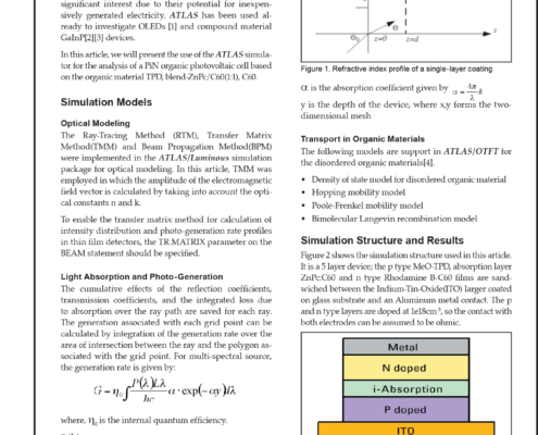 https://silvaco.com/wp-content/uploads/simulationstandard/simstd_aug_2007_a3.jpg
1669
1344
Erick Castellon
/wp-content/uploads/2019/11/silvaco-logo.png
Erick Castellon2007-08-01 00:03:572021-07-16 21:46:31Simulation of an Organic Photovoltaic Cell (OPC) Using Atlas
https://silvaco.com/wp-content/uploads/simulationstandard/simstd_aug_2007_a3.jpg
1669
1344
Erick Castellon
/wp-content/uploads/2019/11/silvaco-logo.png
Erick Castellon2007-08-01 00:03:572021-07-16 21:46:31Simulation of an Organic Photovoltaic Cell (OPC) Using Atlas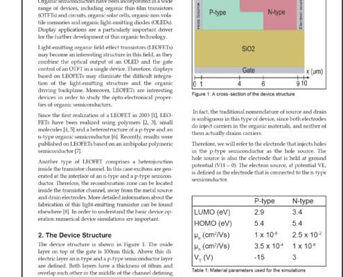 https://silvaco.com/wp-content/uploads/simulationstandard/simstd_aug_2007_a2.jpg
1669
1344
Erick Castellon
/wp-content/uploads/2019/11/silvaco-logo.png
Erick Castellon2007-08-01 00:02:292021-07-16 21:46:32Two-Dimensional Atlas Device Simulation of an Organic Light-Emitting Field-Effect Transistor Using a Heterostructure Inside the Transistor Channel
https://silvaco.com/wp-content/uploads/simulationstandard/simstd_aug_2007_a2.jpg
1669
1344
Erick Castellon
/wp-content/uploads/2019/11/silvaco-logo.png
Erick Castellon2007-08-01 00:02:292021-07-16 21:46:32Two-Dimensional Atlas Device Simulation of an Organic Light-Emitting Field-Effect Transistor Using a Heterostructure Inside the Transistor Channel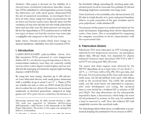 https://silvaco.com/wp-content/uploads/simulationstandard/simstd_may_2007_a2-e1611193444254.jpg
800
644
Erick Castellon
/wp-content/uploads/2019/11/silvaco-logo.png
Erick Castellon2007-05-01 00:02:262021-07-16 21:46:32Electrical Stress Degradation of Small-Grain Polysilicon Thin-Film Transistors
https://silvaco.com/wp-content/uploads/simulationstandard/simstd_may_2007_a2-e1611193444254.jpg
800
644
Erick Castellon
/wp-content/uploads/2019/11/silvaco-logo.png
Erick Castellon2007-05-01 00:02:072021-07-16 21:46:46Trapping Effects in the Transient Response of AlGaN/GaN HEMT Devices
https://silvaco.com/wp-content/uploads/simulationstandard/simstd_may_2007_a2-e1611193444254.jpg
800
644
Erick Castellon
/wp-content/uploads/2019/11/silvaco-logo.png
Erick Castellon2007-05-01 00:02:262021-07-16 21:46:32Electrical Stress Degradation of Small-Grain Polysilicon Thin-Film Transistors
https://silvaco.com/wp-content/uploads/simulationstandard/simstd_may_2007_a2-e1611193444254.jpg
800
644
Erick Castellon
/wp-content/uploads/2019/11/silvaco-logo.png
Erick Castellon2007-05-01 00:02:072021-07-16 21:46:46Trapping Effects in the Transient Response of AlGaN/GaN HEMT Devices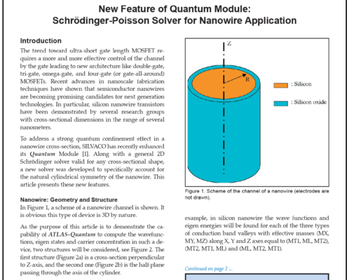 https://silvaco.com/wp-content/uploads/simulationstandard/simstd_may_2007_a1.jpg
1669
1252
Erick Castellon
/wp-content/uploads/2019/11/silvaco-logo.png
Erick Castellon2007-05-01 00:01:242021-07-16 21:46:46New Feature of Quantum Module: Schrödinger-Poisson Solver for Nanowire Application
https://silvaco.com/wp-content/uploads/simulationstandard/simstd_may_2007_a1.jpg
1669
1252
Erick Castellon
/wp-content/uploads/2019/11/silvaco-logo.png
Erick Castellon2007-05-01 00:01:242021-07-16 21:46:46New Feature of Quantum Module: Schrödinger-Poisson Solver for Nanowire Application https://silvaco.com/wp-content/uploads/simulationstandard/simstd_feb_2007_hints-e1611194185247.jpg
800
644
Erick Castellon
/wp-content/uploads/2019/11/silvaco-logo.png
Erick Castellon2007-02-01 00:04:442021-07-16 21:46:47How Can I significantly Reduce Circuit Parasitics Netlist Extraction Time?
https://silvaco.com/wp-content/uploads/simulationstandard/simstd_feb_2007_hints-e1611194185247.jpg
800
644
Erick Castellon
/wp-content/uploads/2019/11/silvaco-logo.png
Erick Castellon2007-02-01 00:04:442021-07-16 21:46:47How Can I significantly Reduce Circuit Parasitics Netlist Extraction Time?