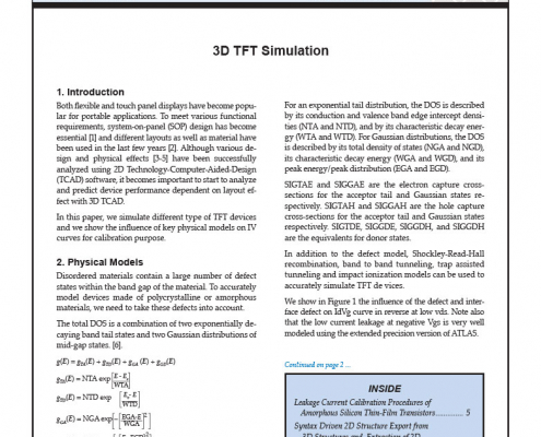
3D TFT Simulation
Both flexible and touch panel displays have become popular for portable applications. To meet various functional requirements, system-on-panel (SOP) design has become essential [1] and different layouts as well as material have been used in the last few years [2]. Although various design and physical effects [3-5] have been successfully analyzed using 2D Technology-Computer-Aided-Design (TCAD) software, it becomes important to start to analyze and predict device performance dependent on layout effect with 3D TCAD.
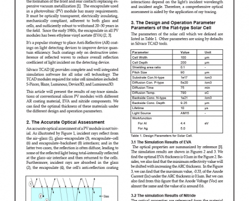
The Studies of Anti-Reflective (AR) Coatings Effects for Solar Cell by Using Silvaco TCAD Tools
In 1975, screen printing was first applied to solar cells for the formation of the front and rear contacts replacing expensive vacuum metallization [1]. The encapsulate used in a photovoltaic (PV) module has many requirements. It must be optically transparent, electrically insulating, mechanically compliant, adherent to both glass and cells, and sufficiently robust to withstand 20–30 years in the field. Since the early 1980s, the encapsulate in all PV modules has been ethylene vinyl acetate (EVA) [2, 3].
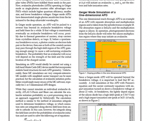
Geiger Mode Simulation of Avalanche Photodiodes in ATLAS
Single-photon counting detectors are used in a wide range of applications, including astronomy, optical communications, biological sensors, and military uses. Photomultiplier tubes (PMTs) have fulfilled these needs in the past. Now, avalanche photodiodes (APDs) operating in Geiger mode as single-photon counters offer advantages over PMTs which include higher quantum efficiency, smaller size, and lower breakdown voltages. Geiger mode APDs have demonstrated single-photon sensitivites from the far infrared to the deep ultraviolet wavelengths.
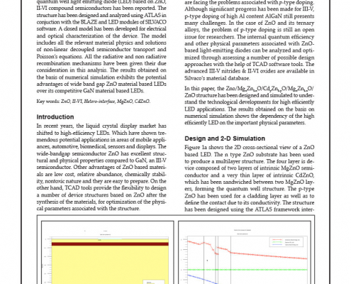
ZnO based LED: A Performance Optimization through TCAD Simulation
In this paper, a two dimensional (2-D) generic model of quantum well light emitting diode (LED) based on ZnO, II-VI compound semiconductors has been reported. The structure has been designed and analyzed using ATLAS in conjuction with the BLAZE and LED modules of SILVACO software. A closed model has been developed for electrical and optical characterization of the device. The model includes all the relevant material physics and solutions of non-linear decoupled semiconductor transport and Poisson’s equations. All the radiative and non radiative recombination mechanisms have been given their due consideration in this analysis. The results obtained on the basis of numerical simulation exhibits the potential advantages of wide band gap ZnO material based LEDs over its competitive GaN material based LEDs.
Normally-off AlGaN/GaN HFET with p-type GaN Gate and AlGaN Buffer
To break through the material limits of Silicon and to realize the drastic performance improvement needed to meet the severe requirements in the future, wide bandgap semiconductors such as SiC and GaN have attracted much attention. AlGaN/GaN HEMTs are generally promising candidates for switching power transistors due to their high breakdown strength and the high current density in the transistor channel giving a low on-state resistance. Further, there exists a high requirement for simulation tools to accurately predict device performance prior to fabrication because of the high inherent cost of the cut-and-try method.
Simulation of Stresses and Mobility Enhancement Factors in 3D Inverter Cell
The analysis and characterization of stress effects have become an integral part of semiconductor technology and device design. In a typical semiconductor process flow the stresses are generated primarily due to volume expansion or contraction of the adjacent materials during temperature variations. Stresses could also be generated during oxidation, silicidation, etching, and deposition processes or due to lattice expansion or contraction after introducing large doses of dopants. Simulation of process induced stresses is an important component of traditional TCAD analysis since these stresses could have adverse or positive effect on individual process steps or on final device characteristics.
High Light Extraction on OLED with Microcavity Effects
OLEDs have been researched for application in display devices due to their considerable advantages. In order to further improve and optimize devices for practical applications, the electrical and optical parts have to be considered.

Modelling of GaN/InGaN Tricolour Multiple Quantum Well Light Emitting Diodes
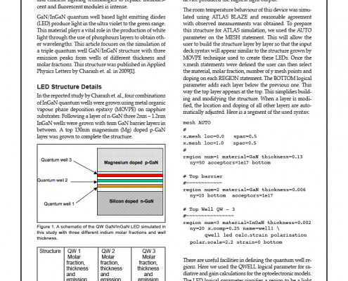
Since lighting is estimated to account for 20% of the world’s electricity consumption, the search for reliable and efficient lighting technologies to replace incandescent and fluorescent modules is intense.
InGaN/GaN Ridge Type with MQW Laser Diode Simulation Using ATLAS
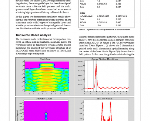
The light source on short wavelenghts has been researched in GaN-based lser diodes (LDs). For high efficiency emitting devices, the wave-guide layer has been investigated to obtain more stable far field patterns and the multi-quantum well layers have been researched as a means of acheiving high quantum efficiency in blue-violet lasers.
Using VICTORY Process to Model Thermal Oxidation of Silicon in O2/HCl Mixtures
The addition of a chlorine species during thermal oxidation of silicon results in improved threshold stability, higher and more uniform oxide dielectric strength and improved junction properties due to lower leakage [1-3]. The effect of HCl addition is to increase the oxidation rate relative to the oxidation rate in dry oxidation ambient (O2), whilst no influence of HCL on the oxidation rate is seen for wet oxidation ambient (H20). The observed increase in oxidation rate is due to:
