Hints, Tips, and Solutions – Defining VWF Curve Target For Curve Calibration
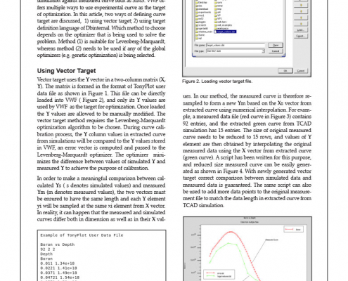
VWF allows a curve as target for optimization. This feature greatly benefits the users who need to calibrate TCAD simulation against measured curve such as SIMS. VWF offers multiple ways to use experimental curve as the target of optimization. In this article, two ways of defining curve target are discussed, 1) using vector target; 2) using target definition language of Dbinternal. Which method to choose depends on the optimizer that is being used to solve the problem. Method (1) is suitable for Levenberg-Marquardt, whereas method (2) needs to be used if any of the global optimizers (e.g. genetic optimization) is being selected.
Hints, Tips, and Solutions – Crop and Slice in the Victory Process 3D Exports
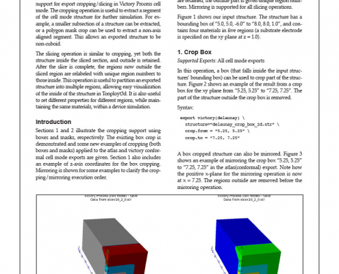
This document is a short guide on the new and existing support for export cropping/slicing in Victory Process cell mode. The cropping operation is useful to extract a segment of the cell mode structure for further simulation. For example, a smaller subsection of a structure can be extracted, or a polygon mask crop can be used to extract a non-axis aligned segment. This allows an exported structure to be non-cuboid.
Hints, Tips and Solutions – Develop your own etch model in Victory Process
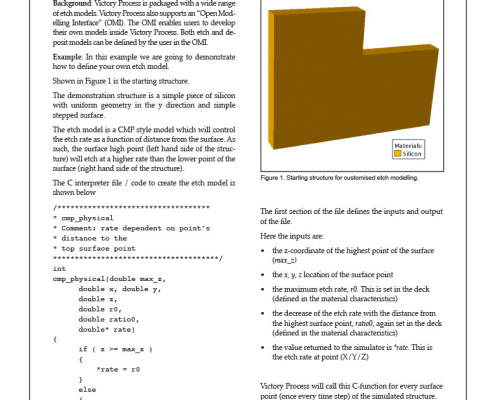
Background: Victory Process is packaged with a wide range of etch models. Victory Process also supports an “Open Modelling Interface” (OMI). The OMI enables users to develop their own models inside Victory Process. Both etch and deposit models can be defined by the user in the OMI.
Simulating Radiation-Induced Shifts in MOSFET Threshold Voltage
Irradiation by energetic particles can degrade semiconductor device performance. The particles involved can be electrons, positrons, neutrons, protons, alpha particles, heavy ions, or high-energy photons. As they pass through a device, these particles interact with the lattice. Energy deposited through these interactions may damage the lattice directly by displacing its atoms, or may result in the creation of electron/hole pairs. A sudden excess of electron/hole pairs may trigger a latchup, possibly damaging the device through overcurrent. Holes generated within an insulator may become trapped there, leading to a gradual accumulation of charge that worsens performance and eventually causes the device to fail. Consideration and modeling of these effects is important when designing semiconductor devices that will be exposed to high-energy radiation.
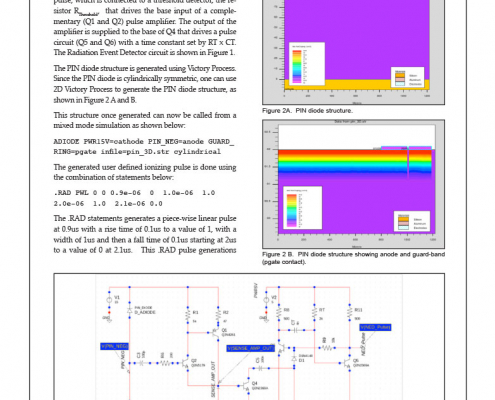
Mixed Mode Radiation Event Detector
A reversed biased PIN diode acts as a radiation event detector, sensing the occurrence of an ionizing radiation pulse, which is connected to a threshold detector, the resistor RThreshold, that drives the base input of a complementary (Q1 and Q2) pulse amplifier. The output of the amplifier is supplied to the base of Q4 that drives a pulse circuit (Q5 and Q6) with a time constant set by RT x CT. The Radiation Event Detector circuit is shown in Figure 1.
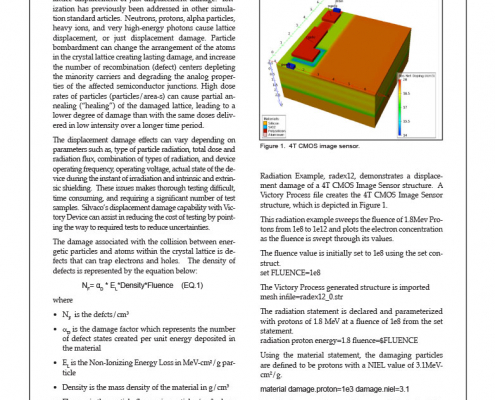
Displacement Damage
Two fundamental damage mechanisms take place when devices are exposed to particle fluences: ionization and lattice displacement or just displacement damage. Ionization has previously been addressed in other simulation standard articles. Neutrons, protons, alpha particles, heavy ions, and very high-energy photons cause lattice displacement, or just displacement damage. Particle bombardment can change the arrangement of the atoms in the crystal lattice creating lasting damage, and increase the number of recombination (defect) centers depleting the minority carriers and degrading the analog properties of the affected semiconductor junctions. High dose rates of particles (particles/area-s) can cause partial annealing (“healing”) of the damaged lattice, leading to a lower degree of damage than with the same doses delivered in low intensity over a longer time period.
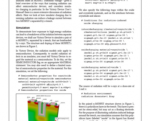
Radiation-Induced Current Leakage Between Two n-MOSFET’s
The Simulation Standard article “Simulating Radiation-Induced Shifts in MOSFET Threshold Voltage”1 gives a brief overview of the ways that ionizing radiation can affect semiconductor devices, and considers insulator charging in particular. In the Victory Device User’s Manual2 there is a more extensive discussion of radiation effects. Here we look at how insulator charging due to ionizing radiation can induce a leakage current between two MOSFET’s separated by a trench.
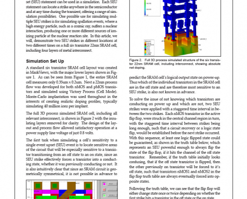
Multiple SEU Strike Simulations on a Six Transistor 20nm SRAM Cell
It is often not realized that more than one Single Event Upset (SEU) statement can be used in a simulation. Each SEU statement can locate a strike anywhere in the semiconductor and at any time during the transient, offering a range of simulation possibilities. One possible use for simulating multiple SEU strikes is for simulating spallation events, where a high energy particle, such as a cosmic ray, suffers a nuclear interaction, producing one or more different sources of ionizing particle at the nuclear reaction site. In this article, we will, demonstrate two SEU strikes in different locations at two different times on a full six transistor 22nm SRAM cell, including four layers of metal interconnect.

The Physics of Single Event Burnout (SEB)
Single Event Burnout in a diode, requires a specific set of circumstances to occur, since there is no intrinsic current gain in the device itself to amplify the currents created by the charge from a single event strike. What has to happen for Single Event Burnout (SEB) to occur in a device with no intrinsic gain, for realistic levels of Linear Energy Transfer (LET), for any given bias is fundamentally simple:
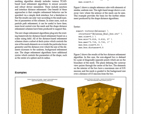
Hints, Tips, and Solutions – Types of 3D Delaunay Shape Refinement in Victory Process
The Victory Process cell mode Delaunay 3D device meshing algorithm already includes various TCAD-based local refinement algorithms to ensure accurate and robust device simulation. These include junction and interface distance refinement. One benefit of these approaches is that complex refinement behavior can be specified via a simple deck interface, but a limitation is that the results can only vary according to the small number of parameters of the schemes. In some cases, such as particle path refinement, it can be useful to have finer, more local control over the mesh and the shape distance refinement schemes have been produced to support this.
