 https://silvaco.com/wp-content/uploads/2020/03/simstd_Q2_2009_hints.jpg
1012
782
Ingrid Schwarz
/wp-content/uploads/2019/11/silvaco-logo.png
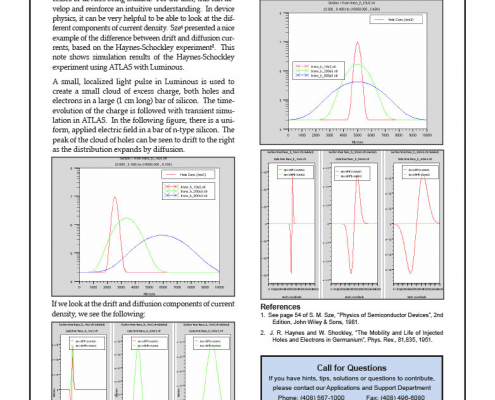
Ingrid Schwarz2009-04-01 16:06:382021-07-08 18:23:29Hints, Tips and Solutions – Visualizing Drift and Diffusion Current Densities
https://silvaco.com/wp-content/uploads/2020/03/simstd_Q2_2009_hints.jpg
1012
782
Ingrid Schwarz
/wp-content/uploads/2019/11/silvaco-logo.png
Ingrid Schwarz2009-04-01 16:06:382021-07-08 18:23:29Hints, Tips and Solutions – Visualizing Drift and Diffusion Current Densities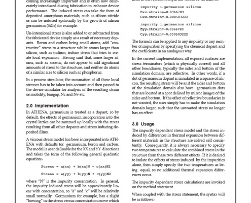 https://silvaco.com/wp-content/uploads/2020/03/simstd_Q2_2009_a4.jpg
1012
782
Ingrid Schwarz
/wp-content/uploads/2019/11/silvaco-logo.png
Ingrid Schwarz2009-04-01 15:59:172021-07-08 18:23:42Simulating SiGe and Impurity Dependent Stress
https://silvaco.com/wp-content/uploads/2020/03/simstd_Q2_2009_a4.jpg
1012
782
Ingrid Schwarz
/wp-content/uploads/2019/11/silvaco-logo.png
Ingrid Schwarz2009-04-01 15:59:172021-07-08 18:23:42Simulating SiGe and Impurity Dependent Stress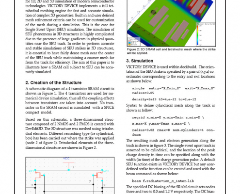 https://silvaco.com/wp-content/uploads/2020/03/simstd_Q2_2009_a3.jpg
1012
782
Ingrid Schwarz
/wp-content/uploads/2019/11/silvaco-logo.png
Ingrid Schwarz2009-04-01 15:53:352021-07-08 18:23:43Physical 3D Single Event Upset Simulation of a SRAM Cell with VICTORY DEVICE and SmartSpice
https://silvaco.com/wp-content/uploads/2020/03/simstd_Q2_2009_a3.jpg
1012
782
Ingrid Schwarz
/wp-content/uploads/2019/11/silvaco-logo.png
Ingrid Schwarz2009-04-01 15:53:352021-07-08 18:23:43Physical 3D Single Event Upset Simulation of a SRAM Cell with VICTORY DEVICE and SmartSpice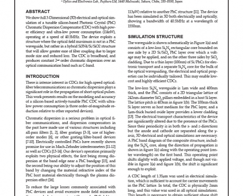 https://silvaco.com/wp-content/uploads/2020/03/simstd_Q2_2009_a2.jpg
1012
782
Ingrid Schwarz
/wp-content/uploads/2019/11/silvaco-logo.png
Ingrid Schwarz2009-04-01 15:49:482021-07-08 18:23:43Electrically Controlled Silicon-based Photonic Crystal Chromatic Dispersion Compensator with Ultra Low Power Consumption
https://silvaco.com/wp-content/uploads/2020/03/simstd_Q2_2009_a2.jpg
1012
782
Ingrid Schwarz
/wp-content/uploads/2019/11/silvaco-logo.png
Ingrid Schwarz2009-04-01 15:49:482021-07-08 18:23:43Electrically Controlled Silicon-based Photonic Crystal Chromatic Dispersion Compensator with Ultra Low Power Consumption https://silvaco.com/wp-content/uploads/2020/03/simstd_Q2_2009_a1.jpg
1012
782
Ingrid Schwarz
/wp-content/uploads/2019/11/silvaco-logo.png
Ingrid Schwarz2009-04-01 15:34:162021-07-08 18:23:44SONOS/SANOS Simulation in ATLAS
https://silvaco.com/wp-content/uploads/2020/03/simstd_Q2_2009_a1.jpg
1012
782
Ingrid Schwarz
/wp-content/uploads/2019/11/silvaco-logo.png
Ingrid Schwarz2009-04-01 15:34:162021-07-08 18:23:44SONOS/SANOS Simulation in ATLAS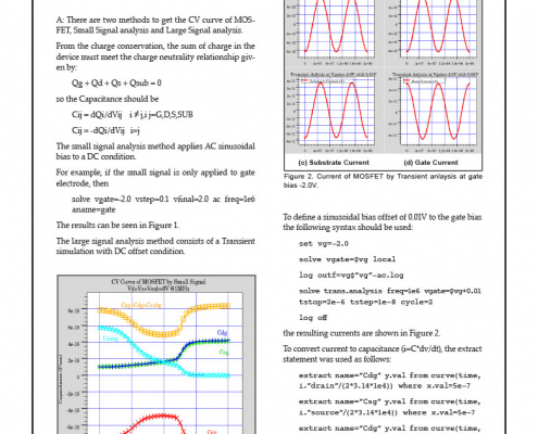 https://silvaco.com/wp-content/uploads/2020/03/simstd_Q1_2009_hints.jpg
1012
782
Ingrid Schwarz
/wp-content/uploads/2019/11/silvaco-logo.png
Ingrid Schwarz2009-01-01 15:18:442021-07-08 18:23:44Hints, Tips and Solutions – Determining the CV Curve and Terminal Currents of a MOSFET
https://silvaco.com/wp-content/uploads/2020/03/simstd_Q1_2009_hints.jpg
1012
782
Ingrid Schwarz
/wp-content/uploads/2019/11/silvaco-logo.png
Ingrid Schwarz2009-01-01 15:18:442021-07-08 18:23:44Hints, Tips and Solutions – Determining the CV Curve and Terminal Currents of a MOSFET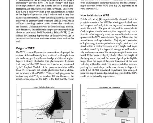 https://silvaco.com/wp-content/uploads/2020/03/simstd_Q1_2009_a5.jpg
1012
782
Ingrid Schwarz
/wp-content/uploads/2019/11/silvaco-logo.png
Ingrid Schwarz2009-01-01 15:03:112021-07-08 18:24:09Minimization of Well-Proximity Effect by Means of 2D and 3D Monte Carlo Simulation of Retrograde Well Implantation
https://silvaco.com/wp-content/uploads/2020/03/simstd_Q1_2009_a5.jpg
1012
782
Ingrid Schwarz
/wp-content/uploads/2019/11/silvaco-logo.png
Ingrid Schwarz2009-01-01 15:03:112021-07-08 18:24:09Minimization of Well-Proximity Effect by Means of 2D and 3D Monte Carlo Simulation of Retrograde Well Implantation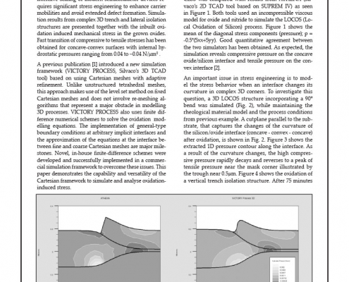 https://silvaco.com/wp-content/uploads/2020/03/simstd_Q1_2009_a4.jpg
1012
782
Ingrid Schwarz
/wp-content/uploads/2019/11/silvaco-logo.png
Ingrid Schwarz2009-01-01 15:00:342021-07-08 18:24:103D Simulation of Oxidation Induced Stress Using Cartesian Meshes with Adaptive Refinement
https://silvaco.com/wp-content/uploads/2020/03/simstd_Q1_2009_a4.jpg
1012
782
Ingrid Schwarz
/wp-content/uploads/2019/11/silvaco-logo.png
Ingrid Schwarz2009-01-01 15:00:342021-07-08 18:24:103D Simulation of Oxidation Induced Stress Using Cartesian Meshes with Adaptive Refinement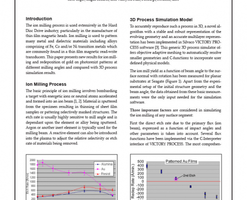 https://silvaco.com/wp-content/uploads/2020/03/simstd_Q1_2009_a3.jpg
1012
782
Ingrid Schwarz
/wp-content/uploads/2019/11/silvaco-logo.png
Ingrid Schwarz2009-01-01 14:57:342021-07-08 18:24:103D Simulation of Ion Milling for Mass Storage Applications
https://silvaco.com/wp-content/uploads/2020/03/simstd_Q1_2009_a3.jpg
1012
782
Ingrid Schwarz
/wp-content/uploads/2019/11/silvaco-logo.png
Ingrid Schwarz2009-01-01 14:57:342021-07-08 18:24:103D Simulation of Ion Milling for Mass Storage Applications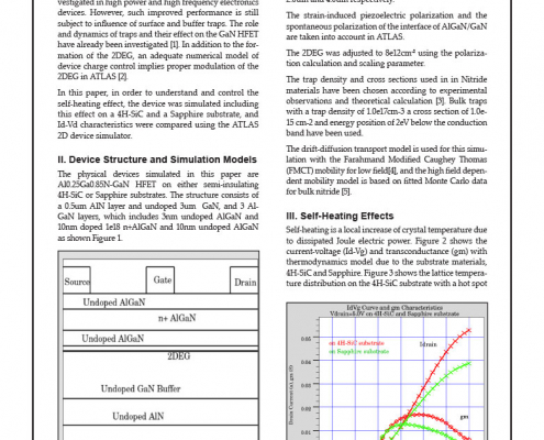 https://silvaco.com/wp-content/uploads/2020/03/simstd_Q1_2009_a2.jpg
1012
782
Ingrid Schwarz
/wp-content/uploads/2019/11/silvaco-logo.png
Ingrid Schwarz2009-01-01 14:46:592021-07-08 18:24:11Self-Heating effect Simulation of GaN HFET Devices – 4H-SiC and Sapphire Substrate Comparison
https://silvaco.com/wp-content/uploads/2020/03/simstd_Q1_2009_a2.jpg
1012
782
Ingrid Schwarz
/wp-content/uploads/2019/11/silvaco-logo.png
Ingrid Schwarz2009-01-01 14:46:592021-07-08 18:24:11Self-Heating effect Simulation of GaN HFET Devices – 4H-SiC and Sapphire Substrate Comparison