 https://silvaco.com/wp-content/uploads/2020/03/simstd_Q4_2015_hints.jpg
1012
782
Ingrid Schwarz
/wp-content/uploads/2019/11/silvaco-logo.png
Ingrid Schwarz2015-10-01 10:24:532021-07-08 18:17:43Hints, Tips and Solutions – Create scalable devices with Victory Process
https://silvaco.com/wp-content/uploads/2020/03/simstd_Q4_2015_hints.jpg
1012
782
Ingrid Schwarz
/wp-content/uploads/2019/11/silvaco-logo.png
Ingrid Schwarz2015-10-01 10:24:532021-07-08 18:17:43Hints, Tips and Solutions – Create scalable devices with Victory Process https://silvaco.com/wp-content/uploads/2020/03/simstd_Q3_2015_a3.jpg
1012
782
Ingrid Schwarz
/wp-content/uploads/2019/11/silvaco-logo.png
Ingrid Schwarz2015-07-01 18:15:062021-07-08 18:17:44Improvements and Features of the Updated DeckBuild 2 GUI
https://silvaco.com/wp-content/uploads/2020/03/simstd_Q3_2015_a3.jpg
1012
782
Ingrid Schwarz
/wp-content/uploads/2019/11/silvaco-logo.png
Ingrid Schwarz2015-07-01 18:15:062021-07-08 18:17:44Improvements and Features of the Updated DeckBuild 2 GUI https://silvaco.com/wp-content/uploads/2020/03/simstd_Q3_2015_a2.jpg
1012
782
Ingrid Schwarz
/wp-content/uploads/2019/11/silvaco-logo.png
Ingrid Schwarz2015-07-01 18:12:462021-07-08 18:17:44Performance Improvement by MPI Parallelization in 3D Device Simulation
https://silvaco.com/wp-content/uploads/2020/03/simstd_Q3_2015_a2.jpg
1012
782
Ingrid Schwarz
/wp-content/uploads/2019/11/silvaco-logo.png
Ingrid Schwarz2015-07-01 18:12:462021-07-08 18:17:44Performance Improvement by MPI Parallelization in 3D Device Simulation https://silvaco.com/wp-content/uploads/2020/03/simstd_Q3_2015_a1.jpg
1012
782
Ingrid Schwarz
/wp-content/uploads/2019/11/silvaco-logo.png
Ingrid Schwarz2015-07-01 18:03:202021-07-08 18:17:58Electrical Simulation of Liquid Crystals
https://silvaco.com/wp-content/uploads/2020/03/simstd_Q3_2015_a1.jpg
1012
782
Ingrid Schwarz
/wp-content/uploads/2019/11/silvaco-logo.png
Ingrid Schwarz2015-07-01 18:03:202021-07-08 18:17:58Electrical Simulation of Liquid Crystals https://silvaco.com/wp-content/uploads/2020/03/simstd_Q3_2015_hints.jpg
1012
782
Ingrid Schwarz
/wp-content/uploads/2019/11/silvaco-logo.png
Ingrid Schwarz2015-07-01 10:16:512021-07-08 18:17:58Hints, Tips and Solutions – Local conformal mesh refinement in Victory Process
https://silvaco.com/wp-content/uploads/2020/03/simstd_Q3_2015_hints.jpg
1012
782
Ingrid Schwarz
/wp-content/uploads/2019/11/silvaco-logo.png
Ingrid Schwarz2015-07-01 10:16:512021-07-08 18:17:58Hints, Tips and Solutions – Local conformal mesh refinement in Victory Process https://silvaco.com/wp-content/uploads/2020/03/simstd_Q2_2015_a3.jpg
1012
782
Ingrid Schwarz
/wp-content/uploads/2019/11/silvaco-logo.png
Ingrid Schwarz2015-04-01 17:56:232021-07-08 18:17:59Radiant: GUI-based Design Software for Performing Simulations of Optoelectronic Thin Film Devices Such as LED and OLED
https://silvaco.com/wp-content/uploads/2020/03/simstd_Q2_2015_a3.jpg
1012
782
Ingrid Schwarz
/wp-content/uploads/2019/11/silvaco-logo.png
Ingrid Schwarz2015-04-01 17:56:232021-07-08 18:17:59Radiant: GUI-based Design Software for Performing Simulations of Optoelectronic Thin Film Devices Such as LED and OLED https://silvaco.com/wp-content/uploads/2020/03/simstd_Q2_2015_a2.jpg
1012
782
Ingrid Schwarz
/wp-content/uploads/2019/11/silvaco-logo.png
Ingrid Schwarz2015-04-01 17:54:132021-07-08 18:17:59Optimizing Solar Cell Top Metal Contact Design Introduction
https://silvaco.com/wp-content/uploads/2020/03/simstd_Q2_2015_a2.jpg
1012
782
Ingrid Schwarz
/wp-content/uploads/2019/11/silvaco-logo.png
Ingrid Schwarz2015-04-01 17:54:132021-07-08 18:17:59Optimizing Solar Cell Top Metal Contact Design Introduction https://silvaco.com/wp-content/uploads/2020/03/simstd_Q2_2015_a1.jpg
1012
782
Ingrid Schwarz
/wp-content/uploads/2019/11/silvaco-logo.png
Ingrid Schwarz2015-04-01 17:51:482021-07-08 18:18:00Vertical LOCOS Power Devices in Victory Process: From 3D Process and Electrical Optimisation to High Speed, Full Chip Process Emulation
https://silvaco.com/wp-content/uploads/2020/03/simstd_Q2_2015_a1.jpg
1012
782
Ingrid Schwarz
/wp-content/uploads/2019/11/silvaco-logo.png
Ingrid Schwarz2015-04-01 17:51:482021-07-08 18:18:00Vertical LOCOS Power Devices in Victory Process: From 3D Process and Electrical Optimisation to High Speed, Full Chip Process Emulation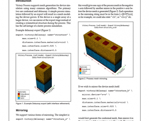 https://silvaco.com/wp-content/uploads/2020/03/simstd_Q2_2015_hints.jpg
1012
782
Ingrid Schwarz
/wp-content/uploads/2019/11/silvaco-logo.png
Ingrid Schwarz2015-04-01 10:58:582021-07-08 18:18:13Hints, Tips and Solutions – Mirror 3D structures in Victory Process
https://silvaco.com/wp-content/uploads/2020/03/simstd_Q2_2015_hints.jpg
1012
782
Ingrid Schwarz
/wp-content/uploads/2019/11/silvaco-logo.png
Ingrid Schwarz2015-04-01 10:58:582021-07-08 18:18:13Hints, Tips and Solutions – Mirror 3D structures in Victory Process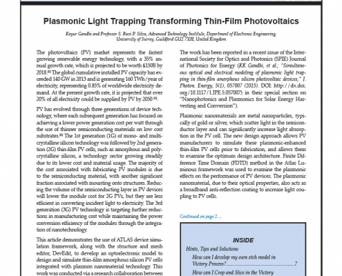 https://silvaco.com/wp-content/uploads/2020/03/simstd_Q1_2015_a2.jpg
1012
782
Ingrid Schwarz
/wp-content/uploads/2019/11/silvaco-logo.png
Ingrid Schwarz2015-01-01 16:59:362021-07-08 18:18:14Plasmonic Light Trapping Transforming Thin-Film Photovoltaics
https://silvaco.com/wp-content/uploads/2020/03/simstd_Q1_2015_a2.jpg
1012
782
Ingrid Schwarz
/wp-content/uploads/2019/11/silvaco-logo.png
Ingrid Schwarz2015-01-01 16:59:362021-07-08 18:18:14Plasmonic Light Trapping Transforming Thin-Film Photovoltaics