Simulating the Source of Polarization Charge in AlGaN/GaN HFETs
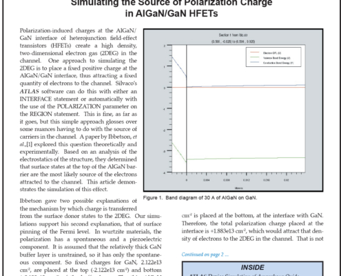
Polarization-induced charges at the AlGaN/GaN interface of heterojunction field-effect transistors (HFETs) create a high density, two-dimensional electron gas (2DEG) in the channel. One approach to simulating the 2DEG is to place a fixed positive charge at the AlGaN/GaN interface, thus attracting a fixed quantity of electrons to the channel. Silvaco’s ATLAS software can do this with either an INTERFACE statement or automatically with the use of the POLARIZATION parameter on the REGION statement. This is fine, as far as it goes, but this simple approach glosses over some nuances having to do with the source of carriers in the channel. A paper by Ibbetson, et al.,[1] explored this question theoretically and experimentally.
Interconnect Parasitic Extraction of BiCMOS Cell Using Silvaco Clever
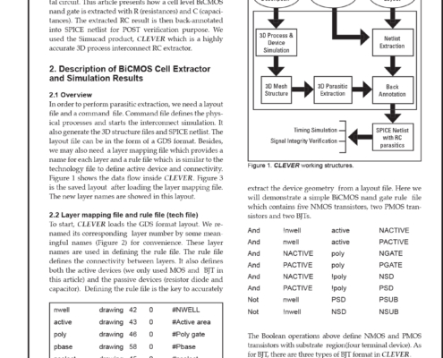
Interconnect parasitic effects play a very important role in modern integrated circuit design, especially for digital circuit. This article presents how a cell level BiCMOS nand gate is extracted with R (resistances) and C (capacitances). The extracted RC result is then back-annotated into SPICE netlist for POST verification purpose. We used the Silvaco product, CLEVER which is a highly accurate 3D process interconnect RC extractor.
Evaluating of the Avalanche Failure of Power MOSFETs using Atlas
Introduction
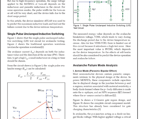
Power MOSFETs are widely used with an inductive load for S/W power supplies, DC-DC converters, and so on. But due to high frequency operation, the surge voltage applied to the MOSFETs at turn-off depends on the inductance and parasitic inductance in the circuit. For some operation modes, the pulse width for the turn-on or off will be very short, and the device fails due to the short surge period.
Comparison of 3-Dimensional Quantum Effects in Nano Devices Using the Atlas 3D BQP Model
Introduction
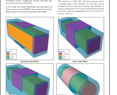
With the MOSFET gate lengths scaling down to sub-20nms many kinds of devices have been proposed and researched such as double-gate, tri-gate, four-gate and gate-all-around (wire) MOSFETs.
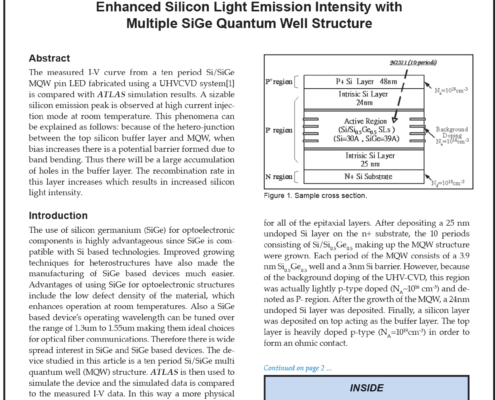
Enhanced Silicon Light Emission Intensity with Multiple SiGe Quantum Well Structure
Abstract
The measured I-V curve from a ten period Si/SiGe MQW pin LED fabricated using a UHVCVD system is compared with ATLAS simulation results. A sizable silicon emission peak is observed at high current injection mode at room temperature. This phenomena can be explained as follows: because of the hetero-junction between the top silicon buffer layer and MQW, when bias increases there is a potential barrier formed due to band bending. Thus there will be a large accumulation of holes in the buffer layer. The recombination rate in this layer increases which results in increased silicon light intensity.
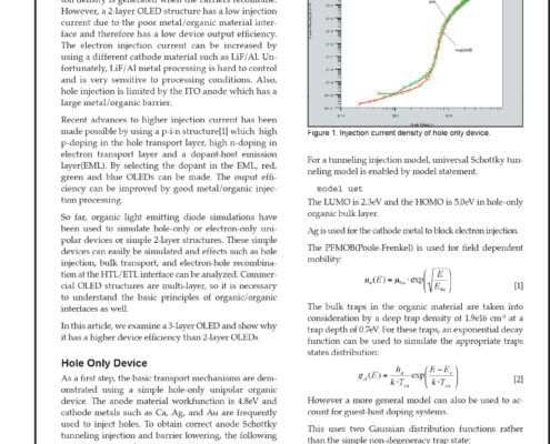
Multi-layer Organic Light Emitting Diode Simulation
A conventional 2 layer organic light emitting diode consists of a Hole Ttransport Layer (HTL) and an electron transport layer (ETL). A good OLED structure requires sufficient carrier injection so that large exciton density is generated when the carriers recombine. However, a 2-layer OLED structure has a low injection current due to the poor metal/organic material interface and therefore has a low device output efficiency. The electron injection current can be increased by using a different cathode material such as LiF/Al. Unfortunately, LiF/Al metal processing is hard to control and is very sensitive to processing conditions. Also, hole injection is limited by the ITO anode which has a large metal/organic barrier.
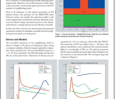
Crosstalk Between Pixels of Organic Photo-Voltaic Devices
For various technological reasons, LEDs and as well as photo-voltaic devices frequently use PEDOT:PSS on top of ITO contacts as a hole injecting or hole collecting layer, respectively. However, due to the presence of this layer, a direct parasitic current path opens up between the ITO contacts of neighboring pixels.
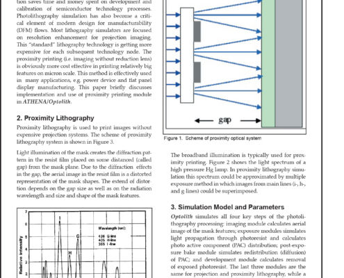
Athena/Optolith Simulation of Proximity Lithography
Photolithography simulation is a very important part of TCAD. Accurate and predictive lithography simulation saves time and money spent on development and calibration of semiconductor technology processes.
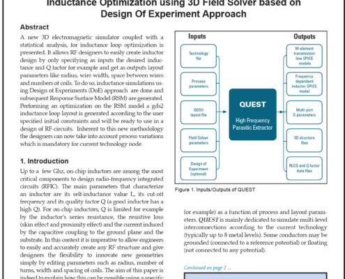
Inductance Optimization using 3D Field Solver based on Design Of Experiment Approach
A new 3D electromagnetic simulator coupled with a statistical analysis, for inductance loop optimization is presented. It allows RF designers to easily create inductor design by only specifying as inputs the desired inductance and Q factor for example and get as outputs layout parameters like radius
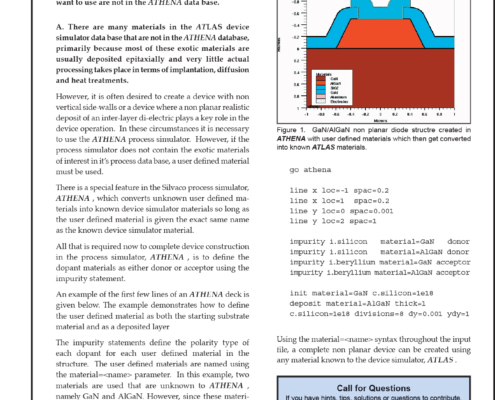
How can I create a non planar structure using III-V materials for Device Analysis
How can I create a non planar structure using III-V materials for Device Analysis when the materials I want to use are not in the ATHENA data base.
