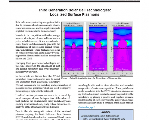
Third Generation Solar Cell Technologies: Localized Surface Plasmons
Solar cells are experiencing a surge in activity due to concerns about sustainability of non-renewable resources and the negative impacts of global warming due to human activity.
Hints, Tips and Solutions – Visualizing Drift and Diffusion Current Densities
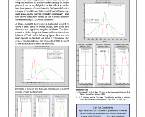
One of the most important features of TCAD simulation is that the TCAD tools encapsulate the physics of the processes or devices being studied. For the user, this can develop and reinforce an intuitive understanding. In device physics, it can be very helpful to be able to look at the different components of current density. Sze1 presented a nice example of the difference between drift and diffusion currents, based on the Haynes-Schockley experiment2. This note shows simulation results of the Haynes-Schockley experiment using ATLAS with Luminous.
Simulating SiGe and Impurity Dependent Stress
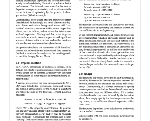
The simulation of stress during device fabrication is becoming increasingly important and is often now deliberately introduced during fabrication to enhance device performance. The induced stress can take the form of deposited amorphous materials, such as silicon nitride or can be induced epitaxially by the growth of silicon germanium (SiGe) for example.
Physical 3D Single Event Upset Simulation of a SRAM Cell with VICTORY DEVICE and SmartSpice
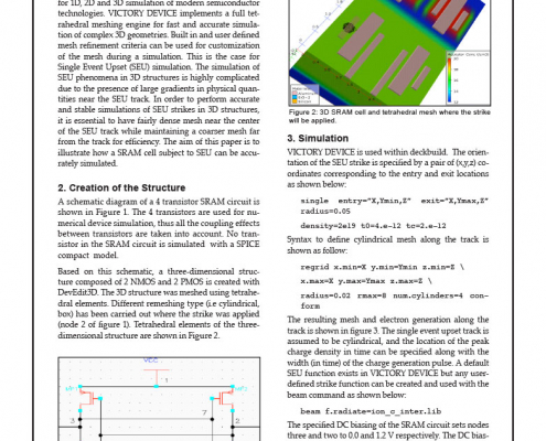
VICTORY DEVICE simulation framework includes tools for 1D, 2D and 3D simulation of modern semiconductor technologies. VICTORY DEVICE implements a full tetrahedral meshing engine for fast and accurate simulation of complex 3D geometries. Built in and user defined mesh refinement criteria can be used for customization of the mesh during a simulation. This is the case for Single Event Upset (SEU) simulation. The simulation of SEU phenomena in 3D structures is highly complicated due to the presence of large gradients in physical quantities near the SEU track. In order to perform accurate and stable simulations of SEU strikes in 3D structures, it is essential to have fairly dense mesh near the center of the SEU track while maintaining a coarser mesh far from the track for efficiency. The aim of this paper is to illustrate how a SRAM cell subject to SEU can be accurately simulated.
Electrically Controlled Silicon-based Photonic Crystal Chromatic Dispersion Compensator with Ultra Low Power Consumption
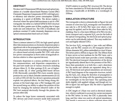
We show full 3-Dimensional (3D) electrical and optical simulation of a tunable silicon-based Photonic Crystal (PhC) Chromatic Dispersion Compensator (CDC) with high power efficiency and ultra-low power consumption (114nW), operating at a speed of 40.5MHz. The device exploits a structure where the optical field maximum is not in a PhC waveguide, but rather in a hybrid Si3N4/Si/SiO2 structure that will allow greater ease of fiber coupling due to larger mode size and reduced loss. The CDC is broadband, and produces constant 2nd order chromatic dispersion over an optical communication band such as C-band.
SONOS/SANOS Simulation in ATLAS
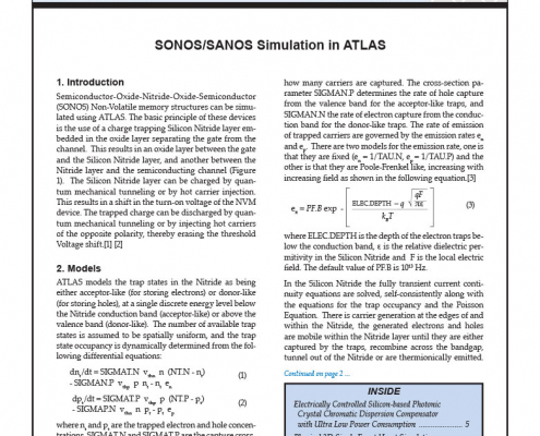
Semiconductor-Oxide-Nitride-Oxide-Semiconductor (SONOS) Non-Volatile memory structures can be simulated using ATLAS. The basic principle of these devices is the use of a charge trapping Silicon Nitride layer embedded in the oxide layer separating the gate from the channel. This results in an oxide layer between the gate and the Silicon Nitride layer, and another between the Nitride layer and the semiconducting channel (Figure 1). The Silicon Nitride layer can be charged by quantum mechanical tunneling or by hot carrier injection. This results in a shift in the turn-on voltage of the NVM device. The trapped charge can be discharged by quantum mechanical tunneling or by injecting hot carriers of the opposite polarity, thereby erasing the threshold Voltage shift.[1] [2]
Hints, Tips and Solutions – Determining the CV Curve and Terminal Currents of a MOSFET
Q: How can I get a CV curve of a MOSFET? And how can I get the current on all terminals?
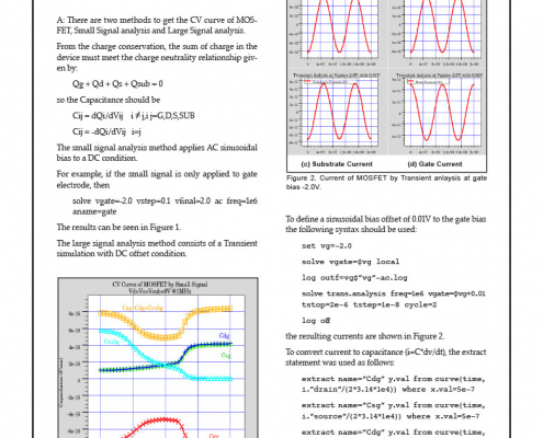
A: There are two methods to get the CV curve of MOSFET, Small Signal analysis and Large Signal analysis.
Minimization of Well-Proximity Effect by Means of 2D and 3D Monte Carlo Simulation of Retrograde Well Implantation
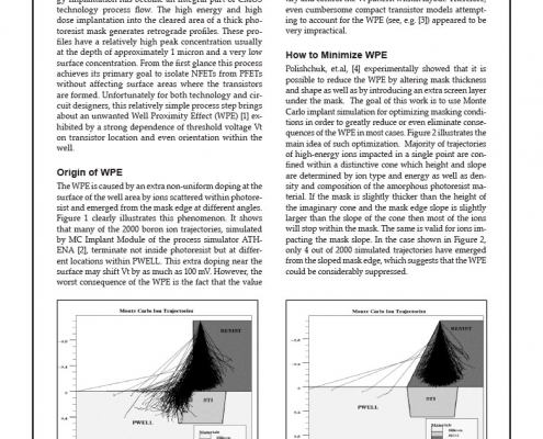
The formation of deep p- and n- wells using high-energy implantation has become an integral part of CMOS technology process flow. The high energy and high dose implantation into the cleared area of a thick photoresist mask generates retrograde profiles. These profiles have a relatively high peak concentration usually at the depth of approximately 1 micron and a very low surface concentration. From the first glance this process achieves its primary goal to isolate NFETs from PFETs without affecting surface areas where the transistors are formed. Unfortunately for both technology and circuit designers, this relatively simple process step brings about an unwanted Well Proximity Effect (WPE) [1] exhibited by a strong dependence of threshold voltage Vt on transistor location and even orientation within the well.
3D Simulation of Oxidation Induced Stress Using Cartesian Meshes with Adaptive Refinement
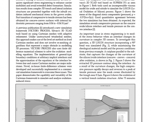
The formation of isolation trenches is one of the key process steps used in power device fabrication. Also the intensive scaling of modern semiconductor devices requires significant stress engineering to enhance carrier mobilities and avoid extended defect formation. Simulation results from complex 3D trench and lateral isolation structures are presented together with the inbuilt oxidation induced mechanical stress in the grown oxides. Fast transition of compressive to tensile stresses has been obtained for concave-convex surfaces with internal hydrostatic pressures ranging from 0.04 to –0.04 N/μm2 .
3D Simulation of Ion Milling for Mass Storage Applications
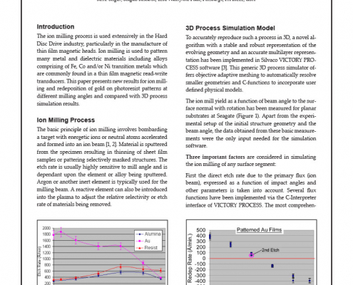
The ion milling process is used extensively in the Hard Disc Drive industry, particularly in the manufacture of thin film magnetic heads. Ion milling is used to pattern many metal and dielectric materials including alloys comprising of Fe, Co and/or Ni transition metals which are commonly found in a thin film magnetic read-write transducers. This paper presents new results for ion milling and redeposition of gold on photoresist patterns at different milling angles and compared with 3D process simulation results.
