 https://silvaco.com/wp-content/uploads/simulationstandard/simstd_jul_2004_a1-e1611194302984.jpg
800
600
Erick Castellon
/wp-content/uploads/2019/11/silvaco-logo.png
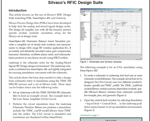
Erick Castellon2004-07-01 00:10:372021-07-08 18:29:40Silvaco’s RFIC Design Suite
https://silvaco.com/wp-content/uploads/simulationstandard/simstd_jul_2004_a1-e1611194302984.jpg
800
600
Erick Castellon
/wp-content/uploads/2019/11/silvaco-logo.png
Erick Castellon2004-07-01 00:10:372021-07-08 18:29:40Silvaco’s RFIC Design Suite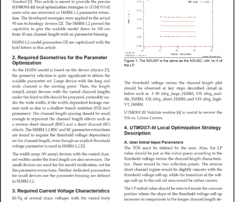 https://silvaco.com/wp-content/uploads/simulationstandard/simstd_jul_2004_a3-e1611194772764.jpg
800
644
Erick Castellon
/wp-content/uploads/2019/11/silvaco-logo.png
Erick Castellon2004-07-01 00:08:282021-07-08 18:29:53HiSIM-1.2 Parameter Extraction with the Revised UTMOST-III Local Optimization Strategies
https://silvaco.com/wp-content/uploads/simulationstandard/simstd_jul_2004_a3-e1611194772764.jpg
800
644
Erick Castellon
/wp-content/uploads/2019/11/silvaco-logo.png
Erick Castellon2004-07-01 00:08:282021-07-08 18:29:53HiSIM-1.2 Parameter Extraction with the Revised UTMOST-III Local Optimization Strategies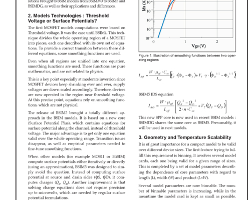 https://silvaco.com/wp-content/uploads/simulationstandard/simstd_jul_2004_a2.jpg
1669
1344
Erick Castellon
/wp-content/uploads/2019/11/silvaco-logo.png
Erick Castellon2004-07-01 00:07:142021-07-08 18:29:54A Family Portrait of the BSIM Models
https://silvaco.com/wp-content/uploads/simulationstandard/simstd_jul_2004_a2.jpg
1669
1344
Erick Castellon
/wp-content/uploads/2019/11/silvaco-logo.png
Erick Castellon2004-07-01 00:07:142021-07-08 18:29:54A Family Portrait of the BSIM Models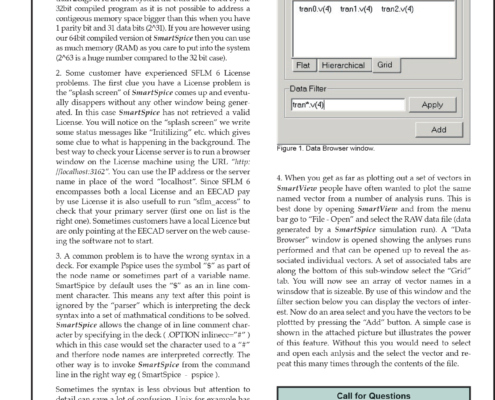 https://silvaco.com/wp-content/uploads/simulationstandard/simstd_jul_2004_hints-e1611193290686.jpg
800
644
Erick Castellon
/wp-content/uploads/2019/11/silvaco-logo.png
Erick Castellon2004-07-01 00:05:492021-07-08 18:29:54Customers are starting to use 64bit machines with large hard drives and Gigs of RAM
https://silvaco.com/wp-content/uploads/simulationstandard/simstd_jul_2004_hints-e1611193290686.jpg
800
644
Erick Castellon
/wp-content/uploads/2019/11/silvaco-logo.png
Erick Castellon2004-07-01 00:05:492021-07-08 18:29:54Customers are starting to use 64bit machines with large hard drives and Gigs of RAM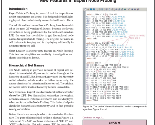 https://silvaco.com/wp-content/uploads/simulationstandard/simstd_jun_2004_a1-e1611194059843.jpg
800
600
Erick Castellon
/wp-content/uploads/2019/11/silvaco-logo.png
Erick Castellon2004-06-01 00:10:082021-07-08 18:29:55New Features in Expert Node Probing
https://silvaco.com/wp-content/uploads/simulationstandard/simstd_jun_2004_a1-e1611194059843.jpg
800
600
Erick Castellon
/wp-content/uploads/2019/11/silvaco-logo.png
Erick Castellon2004-06-01 00:10:082021-07-08 18:29:55New Features in Expert Node Probing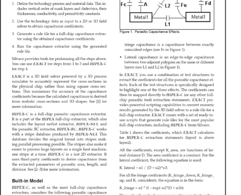 https://silvaco.com/wp-content/uploads/simulationstandard/simstd_jun_2004_a2-e1611194870718.jpg
800
644
Erick Castellon
/wp-content/uploads/2019/11/silvaco-logo.png
Erick Castellon2004-06-01 00:07:262021-07-08 18:29:55Parasitic Capacitance Extraction with Hipex and Exact
https://silvaco.com/wp-content/uploads/simulationstandard/simstd_jun_2004_a2-e1611194870718.jpg
800
644
Erick Castellon
/wp-content/uploads/2019/11/silvaco-logo.png
Erick Castellon2004-06-01 00:07:262021-07-08 18:29:55Parasitic Capacitance Extraction with Hipex and Exact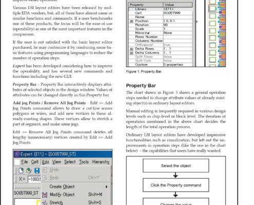 https://silvaco.com/wp-content/uploads/simulationstandard/simstd_jun_2004_a3.jpg
1669
1344
Erick Castellon
/wp-content/uploads/2019/11/silvaco-logo.png
Erick Castellon2004-06-01 00:04:392021-07-08 18:30:33Expert Layout Editor – New Commands Focus On Easier Operation
https://silvaco.com/wp-content/uploads/simulationstandard/simstd_jun_2004_a3.jpg
1669
1344
Erick Castellon
/wp-content/uploads/2019/11/silvaco-logo.png
Erick Castellon2004-06-01 00:04:392021-07-08 18:30:33Expert Layout Editor – New Commands Focus On Easier Operation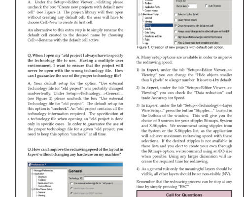 https://silvaco.com/wp-content/uploads/simulationstandard/simstd_jun_2004_hints-e1611194016567.jpg
800
644
Erick Castellon
/wp-content/uploads/2019/11/silvaco-logo.png
Erick Castellon2004-06-01 00:02:262021-07-08 18:30:34Every time I create a new project or library, an empty cell with the same name is created in my project
https://silvaco.com/wp-content/uploads/simulationstandard/simstd_jun_2004_hints-e1611194016567.jpg
800
644
Erick Castellon
/wp-content/uploads/2019/11/silvaco-logo.png
Erick Castellon2004-06-01 00:02:262021-07-08 18:30:34Every time I create a new project or library, an empty cell with the same name is created in my project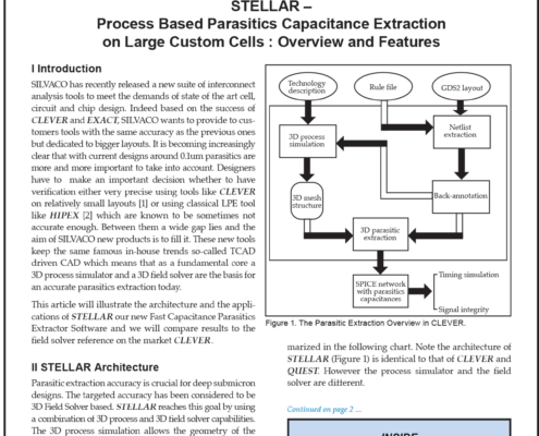 https://silvaco.com/wp-content/uploads/simulationstandard/simstd_may_2004_a1.jpg
1669
1252
Erick Castellon
/wp-content/uploads/2019/11/silvaco-logo.png
Erick Castellon2004-05-01 00:10:092021-07-08 18:30:34STELLAR – Process Based Parasitics Capacitance Extraction on Large Custom Cells
https://silvaco.com/wp-content/uploads/simulationstandard/simstd_may_2004_a1.jpg
1669
1252
Erick Castellon
/wp-content/uploads/2019/11/silvaco-logo.png
Erick Castellon2004-05-01 00:10:092021-07-08 18:30:34STELLAR – Process Based Parasitics Capacitance Extraction on Large Custom Cells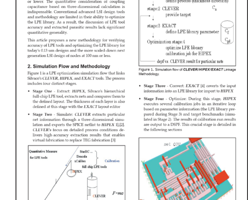 https://silvaco.com/wp-content/uploads/simulationstandard/simstd_may_2004_a3-e1611194214632.jpg
800
644
Erick Castellon
/wp-content/uploads/2019/11/silvaco-logo.png
Erick Castellon2004-05-01 00:07:572021-07-08 18:30:35LPE Optimization with Clever/Hipex/Exact Linkage Methodology
https://silvaco.com/wp-content/uploads/simulationstandard/simstd_may_2004_a3-e1611194214632.jpg
800
644
Erick Castellon
/wp-content/uploads/2019/11/silvaco-logo.png
Erick Castellon2004-05-01 00:07:572021-07-08 18:30:35LPE Optimization with Clever/Hipex/Exact Linkage Methodology