Modeling Quantum Dot Based hyLEDs using Radiant
Radiant is a graphical user interface (GUI) for TCAD simulations which lowers the entry barrier for inexperienced users to doing technology analysis. In particular, the use of guided simulation tools, for both experienced and novice researchers, can speed up the development cycle. Light emitting diodes (LEDs) have caught the attention of the scientific community for many years, especially organic-based light emitting diodes (OLEDs) and the emerging quantum dot-based light emitting diodes (QD-LEDs). As well as the implementation of quantum dot (QD) technology, both organic and inorganic materials have been combined to achieve high-efficiency hybrid light emitting diodes (hyLEDs). This article features the implementation of a simplified 1D simulation of hyLEDs based on QD technology using Radiant software.
hyLED Structure
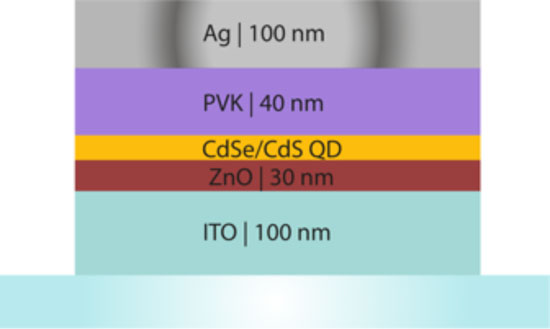
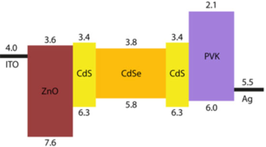
Figure 1. (top) Structure of a layered hybrid light emitting diode (hyLED). (bottom) Band diagram of the same device (displayed values stand for energy (eV)).
hyLEDs receive their name from their hybrid organic-inorganic structure (see Figure 1). The structure of a hyLED is characterized by presenting the electron transport layer (ETL) in contact with the ITO glass (cathode), known as inverted structure. Just above the ETL, a thin polymeric layer is deposited in order to reduce the workfunction of the oxide particles placed immediately below and to inhibit the flow of holes from one contact to the other causing the diode to short circuit. The emissive layer (EML) made of QDs is placed over the ETL. The hole transport layer (HTL) is deposited onto the EML and, if desired, an electron blocker can be placed over it. Finally, metallic contacts are sited on top (anode).
Quantum dots can be either bare form or core-shell form depending on their material distribution (see Figure 2). Their bandgap changes as a function of the size of the particles, hence the emission color can be tuned from red (large size, small bandgap) to blue (small size, large bandgap).

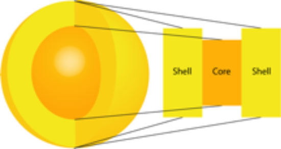
Figure 2. (top) Bare spherical QD. (center) Core-shell spherical QD. (bottom) Schematic energy diagram for 1D-layer approach of the spherical QD (shells behave as potential barriers and core behaves as a quantum well).

Q
Ds present a strong confinement in the three dimensions, so there are no available degrees of freedom for either electrons or holes. However, from the quantum perspective, electrons and holes have different probability functions at the quantum dot site. Figure 3 shows a diagram of the conduction and valence bands at the shell/core/shell interfaces where the wavefunction of electrons and holes are depicted in red. As it can be observed, the probability function of electrons is spread all along the QD (shell and core), with high probability of penetrating the shell barrier. On the other hand, due to their higher effective mass, holes are much more confined at the core of the quantum dot with lower shell penetration. The overlapping of both probability functions governs the probability of the formation of an exciton, which can then relax to its ground state and produce the visible emission.
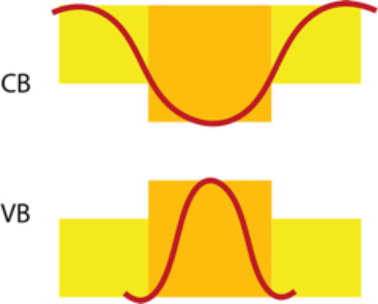
Figure 3. Electron and hole confinement at the QD site. Conduction band (CB) depicts the confinement of electrons and Valence band (VB) depicts the confinement of holes (red lines). The yellow bands represent the QD shell and the orange bands represent the QD core.
Radiative recombination (i.e. light emission) takes place at the core of the quantum dot, due to the strong confinement, which essentially behaves as a quantum well (core) with high potential barriers (shell). Emission and stability can be enhanced by surrounding the core with a large-bandgap barrier shell material.
J-V Characteristics and Power Spectral Density Simulations
Prior to the simulation of a complete device, it is necessary to assemble all the design parameters in Radiant (e.g. material, bandgap, electron affinity). Once all the layers have been set up, the user can select the solving method and the models that best reflect the required carrier transport physics in such simulations, as well as the output results that are desired to obtain. Figure 4 shows the screen of Radiant with the resulting setup. To see the statements used in Deckbuild for the simulation consult the Simulation Standard article.
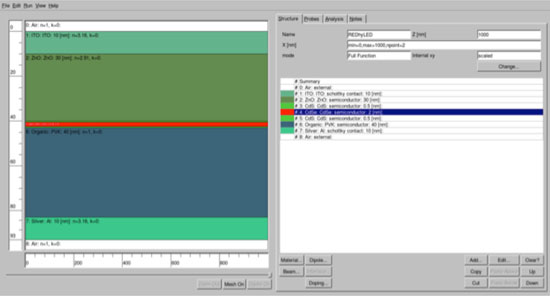
Figure 4. Device designer screen in Radiant. hyLED device setup is displayed.
J-V and Power Spectral Density Results for Different Color of QD
Thanks to the parametric modelling done in this work, it is possible to tune the color of the emission by changing the parameters shown in Table 1.
|
||||||||||||||||
As expected, the J-V curves for all 3 devices with different QD colours and different particle sizes show a negligible variation, meaning a correct modelling and simulation of the technology, as they do not display a shift of the turn-on voltage either.
The power spectral density (PSD) computed from the spontaneous emission of the QD can be seen in Figure 5b. Just by tuning the parameters displayed in Table 1, the wavelength of the emitted photons shift, ranging from red to blue.
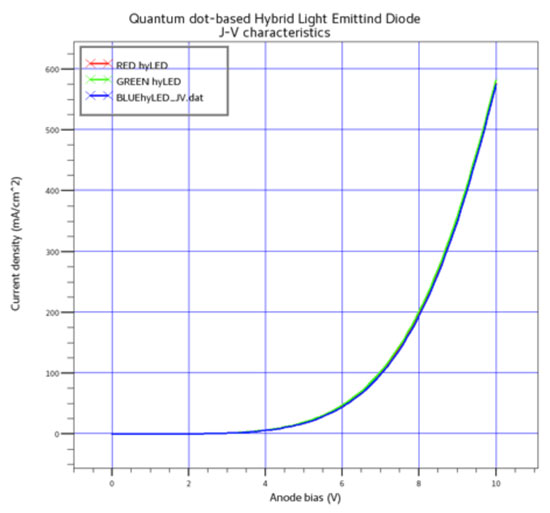
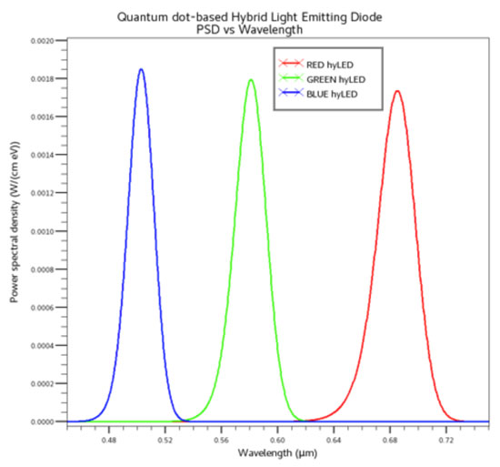
Figure 5. a) J-V characteristics of hyLED devices with different emission colour. b) Power spectral density of hyLED devices with different emission color.
5. Summary
In summary, a simple 1D simulation using a GUI TCAD simulator (Radiant) provides the ability to capture quantum mechanics on quantum dot-based devices using the quantum well approach. It can easily predict the spectral response as a function of the bandgap of the QD and can display the current density of the device, which can reduce the expense of repeated experiments.
