230 Papers on Power Device Simulations using Silvaco TCAD
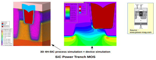
Process and device simulation of a SiC power trench MOSFET.
A quick search of the IEEE Xplore online library gives a list of more than 230 published technical articles on Power Device Simulation using Silvaco TCAD. Here are some recent papers with the authors’ abstracts that cover silicon-carbide (SiC) and Junction-Less Double Gate MOSFET devices. Any mention of ‘we’ or ‘our’ refers to the paper’s authors:
Study of oxide trapping in SiC MOSFETs by means of TCAD simulations, Materials Science in Semiconductor Processing, Volume 97, July 2019, Pages 40-43
“SILICON CARBIDE (SiC) material has attracted substantial attention during the last few years as a promising candidate for making power devices for high-temperature operation and under harsh environments. In spite of the considerable progress in device performance, reliability may be a limiting factor for the introduction of SiC MOSFETs in commercial power devices. One of the major reliability concerns is the instability of the threshold voltage in MOSFETs and, similarly, of the flat-band voltage in capacitors under normal operation conditions. This instability is attributed to trapping of channel electrons in interface and bulk oxide traps.
“The main goal of this work is to investigate how the trapped charges at SiO2/SiC interface influence the C/V curve. In particular, by means of 2-D numerical simulations (SILVACO tools), we could isolate the two different contributions from p-type and n-type doped regions of our MOSFET and we considered both donor and acceptor traps contributions. Then, we compared the simulation results with experimental C/V curves. A good agreement between TCAD simulations and experimental measurements was obtained. So, device simulations can provide a better understanding of such defects at SiO2/SiC interface and we give an insight into the influence of traps, produced during device processing or caused by radiation environment, on the output characteristics of the device.”
Power and Delay Analysis of Junction-Less Double Gate CMOS Inverter in Near and Sub-Threshold Regime, IEEE Electron Devices Kolkata Conference (EDKCON), Nov. 2018
“In this paper, a Junction-Less Double Gate MOSFET (JLDG MOSFET) based CMOS inverter circuit is proposed for ultra-low power applications in the near and sub-threshold regime operations. D.C performances like power and delay of the proposed Inverter have been modeled analytically and analyzed in depth. JLDG MOSFET has promising features to reduce the short channel effects compared to the planner MOSFET because of better gate control mechanism. So, proposed Inverter would be efficacious to offer less power dissipation and higher speed. Impact of supply voltage and the temperature on the power and delay of the Inverter circuits have been detailed here. Extensive simulations have been done using SILVACO TCAD to validate the proposed models. Besides, optimum, supply voltage has been proposed to enhance the efficiency at low supply voltage.”
Investigation on degradation mechanism and optimization for SiC power MOSFETs under long-term short-circuit stress, 2018 IEEE 30th International Symposium on Power Semiconductor Devices and ICs (ISPSD). May 2018
“In this paper, the degradation mechanism of silicon carbide (SiC) power metal-oxide-semiconductor field-effect transistors (MOSFETs) under long-term short-circuit (SC) stress is investigated. With the help of Silvaco TCAD simulations and measurements on degraded parameters, the injection of electrons into gate oxide above channel region of the device is demonstrated to be the dominant degradation mechanism. It results in the positive shift of threshold voltage (V th ) and the increase of on-state resistance (R dson ) under low gate voltage bias condition. Simulated electrical properties of the device with electrons trapped into gate oxide above channel region share similar degradation trend with measured ones, proving the correctness of our analysis. Furthermore, an improved device structure with an additional shallow inverted-doping p-well, which can effectively lower the impact ionization rate (I.I.) along the SiC/SiO 2 interface above channel region during SC process, is proposed to restrict the degradations under long-term SC stress.”
To see more Published Papers on Power Device Simulation using Silvaco TCAD, click on this IEEE Xplore link: https://ieeexplore.ieee.org/search/searchresult.jsp?newsearch=true&queryText=silvaco%20power
