New Model for Simulation of Exposure Process in Complex Nonplanar Resist-Substrate Structures
Introduction
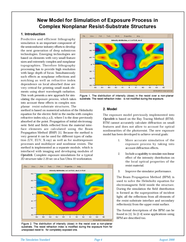
Predictive and efficient lithography simulation is an important component of the semiconductor industry efforts to develop the next generation of deep submicron technologies. Emerging technologies are based on elements with very small feature sizes and extremely complex and nonplanar topographies. Therefore lithography processing has to provide high resolution with large depth of focus. Simultaneously such effects as nonplanar reflections and notching as well as refractive index dependence on local absorbed dose are very critical for printing small mask elements using short wavelength radiation. This work presents a new approach for simulating the exposure process, which takes into account these effects in complex nonplanar resist-substrate structures. The method is based on numerical solution of the Helmholtz equation for the electric field in the media with complex refractive index n(x,y,z,I), where I is the dose previously absorbed at the point. Propagation of initial electromagnetic field and fields reflected from the material interface elements are calculated using the Beam Propagation Method (BMP) [1]. Because the method is very general it can be used for different types of radiation (UV, EUV, X-ray) as well as for multiexposure processes and multilayer and nonlinear resists. The method is implemented as a separate module, which is interfaced with imaging and developing modules of Optolith. Complete exposure simulations for a typical 2D structure take 2-20 sec on a Sun Ultra-10 workstation.


