TCAD Simulation of a Dual Band Monolithic HgCdTe Infrared Photodetector
Introduction
Mercury cadmium telluride (HgCdTe) is a semiconductor material whose material properties are adjustable through altering its constitutive molar fractions. HgCdTe has found extensive use in optical detection, and in particular found wide use in infrared photodetectors over the past few decades. Applications in this area have been the main driving force for research on this material and for a good review see [1]. HgCdTe has an adjustable bandgap whose value can be altered by varying the stociometric ratio of Hg and Cd in the form Hg(1-x)CdxTe. This property enables the detection of multispectral sources through the creation of multispectral infrared detectors of various bandgaps and in particular dual band photodetection [2]. Dual band photodetection in the medium wavelength infrared (MWIR) and long wave infrared atmospheric windows has been performed using HgCdTe photodiodes [e.g. 3] and for a recent example see [4]. This simulation standard will demonstrate the simulation of a dual band HgCdTe monolithic photodetector similar to [4]. The device is suitable for dual band on pixel registered infrared photodetector arrays in the atmospheric transmission window of 3-5µm and 8-12µm.
Device Description and Material Properties
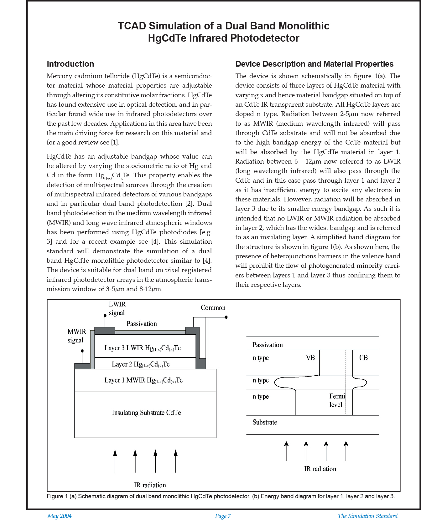
The device is shown schematically in figure 1(a). The device consists of three layers of HgCdTe material with varying x and hence material bandgap situated on top of an CdTe IR transparent substrate. All HgCdTe layers are doped n type. Radiation between 2-5µm now referred to as MWIR (medium wavelength infrared) will pass through CdTe substrate and will not be absorbed due to the high bandgap energy of the CdTe material but will be absorbed by the HgCdTe material in layer 1. Radiation between 6&12µm now referred to as LWIR (long wavelength infrared) will also pass through the CdTe and in this case pass through layer 1 and layer 2 as it has insufficient energy to excite any electrons in these materials. However, radiation will be absorbed in layer 3 due to its smaller energy bandgap. As such it is intended that no LWIR or MWIR radiation be absorbed in layer 2, which has the widest bandgap and is referred to as an insulating layer. A simplified band diagram for the structure is shown in figure 1(b). As shown here, the presence of heterojunctions barriers in the valence band will prohibit the flow of photogenerated minority carriers between layers 1 and layer 3 thus confining them to their respective layers.
The bandgap of HgCdTe is a function of the fraction of Cd in the composite material. A number of equations have been developed to summarize the empirically measured relationship and of popular choice is the expression developed by Hansen et al [5] which describes the energy bands in a parabolic form where
(1)
Here T is the temperature in degrees Kelvin and x is the molar fraction, Eg is the material bandgap in eV and x is the fractional composition value. With varying the value of x, the spectral response can be tailored to detect varying wavelengths. Consequently in order to detect long wavelength radiation, x must be altered accordingly resulting in a semiconductor having a very narrow bandgap. Applied formulae describing effective electron and hole masses are given in equations (2) and (3) respectively. The electron and hole mobilities are given by equations (4) and (5) respectively. The static dielectric constant is given in equation (6).


