Optimization of Select Gate Transistor in Advanced 3D NAND Memory Cell
Jin Cho, Derek Kimpton, Eric Guichard
Silvaco, Inc, Santa Clara, CA, USA
jin.cho@silvaco.com
Abstract—There are several device challenges unique to the select gate transistor in 3D NAND memory cell. It requires low leakage current to prevent read and program disturb problems and it needs to provide enough current during read and erase operation. In this paper, we examined the design optimization of select gate transistor with respect to various device elements including work-function, S/D overlap, and trap density. Finally, we reviewed the path to reduce the channel length of the select gate transistor in conjunction with the role of dummy cells.
Keywords – 3D NAND memory, program/erase operation, program disturb, self-boosting effect
I. INTRODUCTION
Demand for aggressive bit density scaling of 3D NAND memory device is driving more cells per string as well as more string per block. These multiple layers of materials, such as oxide and polysilicon, introduce manufacturing complexity in various NAND process steps, including memory hole, stair step, and slit etch process. It is therefore desirable to reduce the layer thickness while increasing the number of memory cells per string. In addition, the number of dummy cells and gate length of select gate device at the end of memory string play a big role on overall stack thickness. In this paper we studied the role of select gate and dummy cells on memory operation including program disturb and cell operation speed.
II. PROCESS SIMULATION
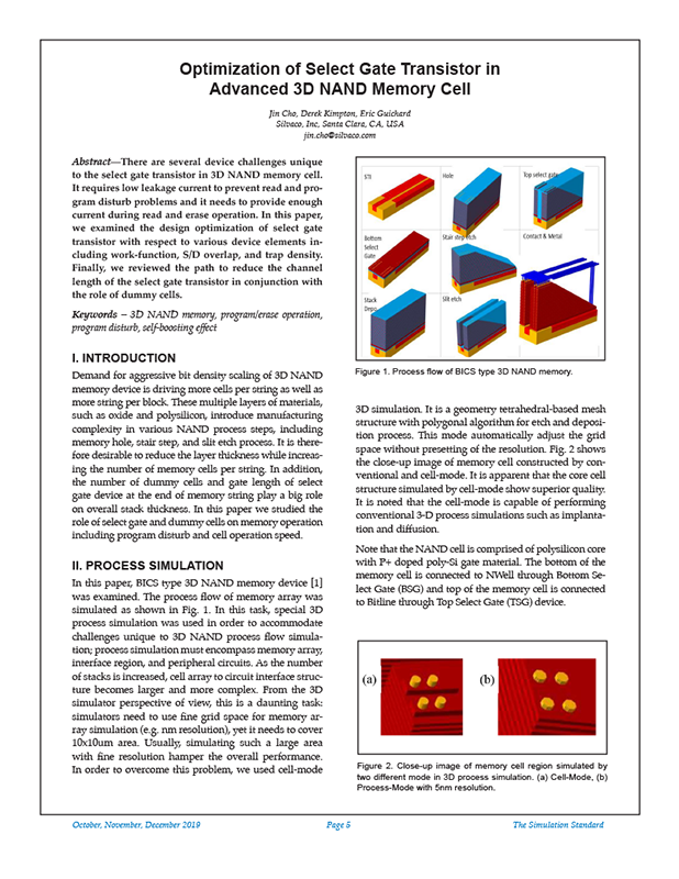
In this paper, BICS type 3D NAND memory device [1] was examined. The process flow of memory array was simulated as shown in Fig. 1. In this task, special 3D process simulation was used in order to accommodate challenges unique to 3D NAND process flow simulation; process simulation must encompass memory array, interface region, and peripheral circuits. As the number of stacks is increased, cell array to circuit interface structure becomes larger and more complex. From the 3D simulator perspective of view, this is a daunting task: simulators need to use fine grid space for memory array simulation (e.g. nm resolution), yet it needs to cover 10x10um area. Usually, simulating such a large area with fine resolution hamper the overall performance. In order to overcome this problem, we used cell-mode 3D simulation. It is a geometry tetrahedral-based mesh structure with polygonal algorithm for etch and deposition process. This mode automatically adjust the grid space without presetting of the resolution. Fig. 2 shows the close-up image of memory cell constructed by conventional and cell-mode. It is apparent that the core cell structure simulated by cell-mode show superior quality. It is noted that the cell-mode is capable of performing conventional 3-D process simulations such as implantation and diffusion.


