TCAD Simulation of a Polysilicon Thin Film Transistor For Active Matrix Liquid Crystal Displays
1 Introduction
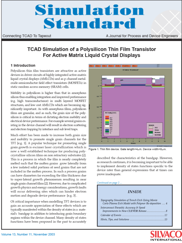
Polysilicon thin film transistors are attractive as active devices in driver circuits of highly integrated active-matrix liquid crystal displays (AMLCDs) and as p-channel metal-oxide-semiconductor field effect transistors (MOSFETs) in static random access memory (SRAM) cells.
Mobility in polysilicon is higher than that in amorphous silicon thus enabling integration and improved performance (e.g. high transconductance) in multi layered MOSFET structures, and low cost AMLCDs which are becoming significantly important. As with amorphous films, polysilicon films are granular, and as such, the grain size of the polysilicon is critical in terms of dictating electron mobility and electrical device performance. For example several grains existing in the device channel will result in electron scattering and electron trapping by interface and sub level traps.
Much effort has been made to increase both grain size and mobility to promote single grain channels for the TFT [e.g. 1]. A popular technique for promoting single grain growth is excimer laser crystallization which is now a well established technique for producing polycrystalline silicon films on non refractory substrates [2]. This is a process in which the film is nearly completely melted such that the molten grains grow laterally from a few isolated solid portions of seed grains that are not included in the molten process. In such a process grains can have diameters far exceeding the film thickness due to super-lateral growth phenomenon resulting in near single grain channel films [2]. However, due to complicated growth physics and energy considerations, growth faults will occur delivering sites which can hinder electron motion and degrade device performance [e.g. 3].


