Automatic Grid Refinement for Thin Material Layer Etching in Process TCAD Simulations
Presented at the 2022 International Conference on Simulation of Semiconductor Processes and Devices (SISPAD)
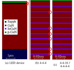 Abstract—The utilization of thin material layers is common in modern semiconductor device fabrication. Subsequent etching steps require an accurate modeling of these thin layers. Although level-set based process TCAD simulations are capable of representing flat thin material layers with sub-grid accuracy, topographical changes during etching processes expose the low underlying grid resolution, which leads to detrimental artifacts. We present a novel algorithm that analyzes the thickness of all material layers and suggests a refined target resolution for local regions of thin layers affected by the etching process. This allows to accurately represent topographical changes in thin layers without refining unaffected regions of the domain. We simulate the fabrication of a light-emitting diode device, where our algorithm is used to automatically predict the optimal resolution for all etched material layers. Our algorithm selects efficient refinement factors to obtain the target resolutions with locally employed hierarchical grids.


