
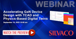
Accelerating GaN Device Design with TCAD and Physics-Based Digital Twins
 Gallium Nitride (GaN) is driving innovation in power electronics, RF systems, and high-frequency applications with superior efficiency, performance, and thermal characteristics compared to. This webinar will start by exploring the key applications and benefits of GaN, providing the foundation for a detailed look at Silvaco’s Victory TCAD workflow for GaN design and optimization.
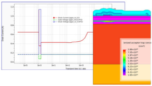
We will demonstrate how Victory TCAD delivers accurate process and device simulations with models tailored to GaN technologies, supported by practical examples like p-GaN gate and vertical GaN device architectures. Attendees will also see how Victory Design of Experiments (DoE) and Victory Analytics enable rapid design exploration and optimization with a digital twin. Finally, we’ll connect device-level simulation to circuit design with SPICE modeling using Utmost IV, completing a streamlined path from GaN concept to system-level validation.
What You Will Learn
- The performance advantages and application areas of Gallium Nitride (GaN) devices.
- How Silvaco’s Victory TCAD workflow enables accurate GaN process and device simulation.
- Practical examples, including p-GaN gate and vertical GaN structures.
- How to use Victory Design of Experiments (DoE) and Victory Analytics to accelerate design optimization.
- How to connect TCAD to circuit-level simulation with SPICE modeling in Utmost IV.
Presenter
Udita Mittal, Field Application Engineer
Udita Mittal joined Silvaco as a Field Applications Engineer within Silvaco’s TCAD division in 2019. She is based out of the India office. Prior to Silvaco, Udita was at Rochester Institute of Technology, Rochester, New York, where she graduated with a Masters in Microelectronics. She is responsible for supporting TCAD for process simulation, training and supporting users in fabrication process simulations for various technologies, with special attention to WBG devices. Udita has worked on simulation of classical and non-classical device simulations. She has worked with material characterization using atomistic modeling and device simulation for 2-D devices.
WHO SHOULD ATTEND:
Process engineers, simulation engineers, fabrication engineers, product managers, and engineering management.
[日本時間]
開催日時:
2025年9月18日
11:00am JST (10:00 Beijing)
6:00pm JST (11:00 Paris)
2025年9月19日
2:00am JST (10:00 Santa Clara)
(各回、同じ内容になります。)
配信: オンライン
言語: 英語