Process and Device Simulation of Field Emission Microtrides
Introduction
One of the most beneficial merits of computer-based experiment using TCAD lies in its capability of a total simulation of the target device. One can consider its novel fabrication process and its device performance at the same time without time consuming and expensive experiments using real wafers. Take field emission microtriodes, for example.
They have been studied for various applications such as field emission displays, high-power and high-frequency devices having high-operating temperature and radiation hardness. In order to fabricate the microtriodes, silicon wafer process technology is preferred because it is suitable in forming a sharp cone structure as its field emitter(1).
Process Simulation
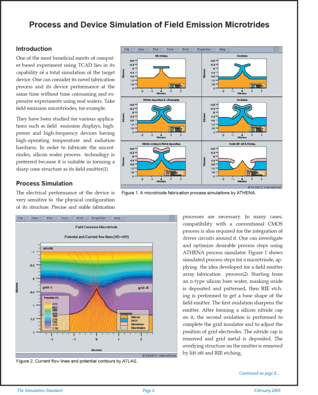
The electrical performance of the device is very sensitive to the physical configuration of its structure. Precise and stable fabrication processes are necessary. In many cases, compatibility with a conventional CMOS process is also required for the integration of driver circuits around it. One can investigate and optimize desirable process steps using ATHENA process simulator. Figure 1 shows simulated process steps for a microtriode, applying the idea developed for a field emitter array fabrication process(2). Starting from an n-type silicon bare wafer, masking oxide is deposited and patterned, then RIE etching is performed to get a base shape of the field emitter. The first oxidation sharpens the emitter. After forming a silicon nitride cap on it, the second oxidation is performed to complete the grid insulator and to adjust the position of grid electrodes. The nitride cap is removed and grid metal is deposited. The overlying structure on the emitter is removed by lift-off and RIE etching.
Device Simulation
Once a desirable structure is obtained by ATHENA process simulation, one can transfer it to ATLAS device simulation directly. In some cases, remeshing suitable for device simulation may be needed to obtain a better convergence and that is easily done using an user-friendly interactive meshing tool DevEdit. In order to estimate the electrical characteristics of the emitter, Fowler-Nordheim equation is used. Figure 2 shows electric potential contours and current flow lines at the anode and grid voltages of 800V and 10V respectively. It can be seen that the current flow lines respond very sensitively to slight irregularities in the shape of the structure. The final results of the emitter current vs. anode voltage curves at various grid voltages are shown in Figure 3.


