Gate Charging Simulation Using ATLAS/MixedMode
Introduction
In modern power devices, the total power loss comprises both a conductive power loss component and a capacitive loss component. As the cell pitch decreases, the conductive loss will decrease while the capacitive loss will increase. Therefore, for small cell pitch the capacitive power loss may be the dominant component of the total power loss in the device.
There is clearly a need for a method that will allow analysis of the capacitive component of the power loss. One technique to do this in a power UMOSFET device is to analyze the gate charging time using ATLAS/MixedMode.
ATLAS/MixedMode is a circuit simulator that can include elements simulated using device simulation, as well as compact circuit models.
Device Structure and Circuit
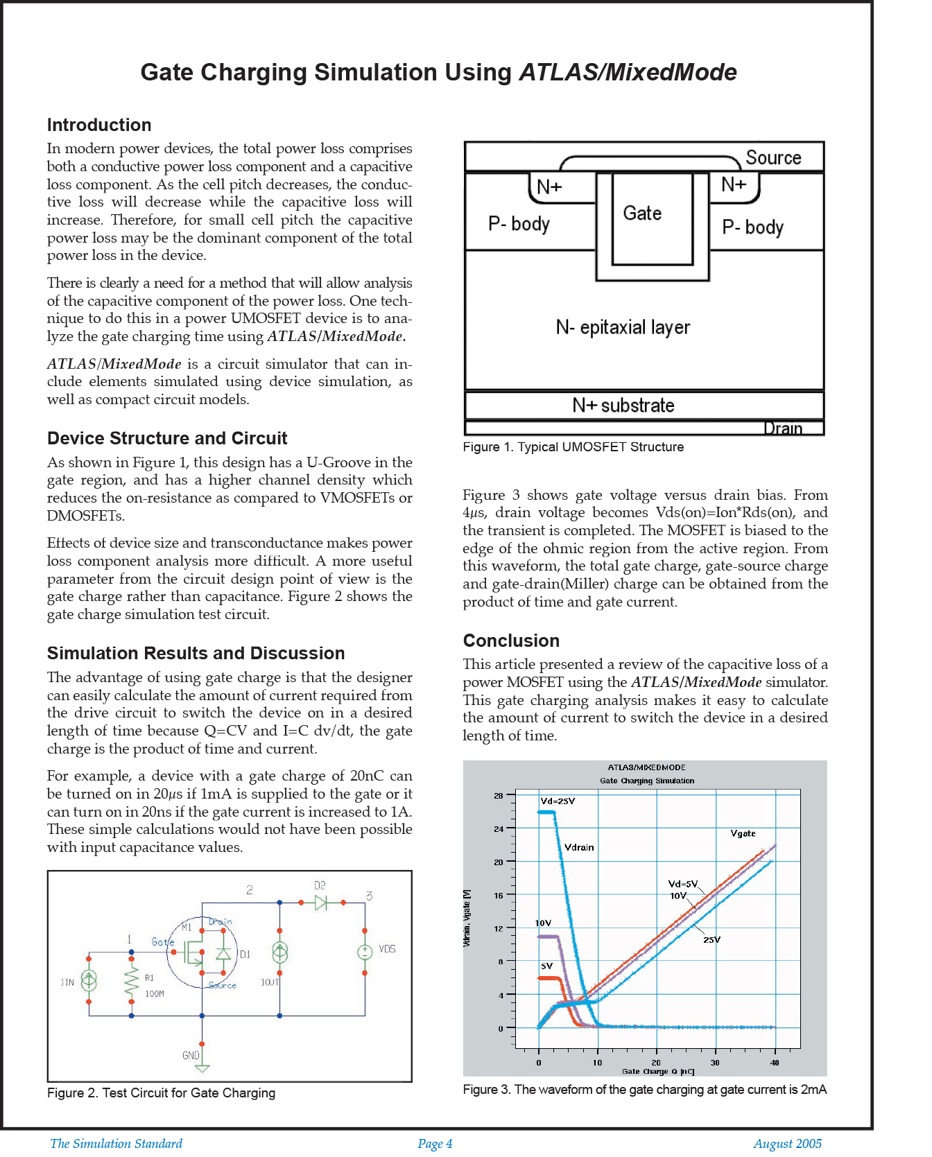
As shown in Figure 1, this design has a U-Groove in the gate region, and has a higher channel density which reduces the on-resistance as compared to VMOSFETs or DMOSFETs.
Effects of device size and transconductance makes power loss component analysis more difficult. A more useful parameter from the circuit design point of view is the gate charge rather than capacitance. Figure 2 shows the gate charge simulation test circuit.


