Enhanced Silicon Light Emission Intensity with Multiple SiGe Quantum Well Structure
Abstract
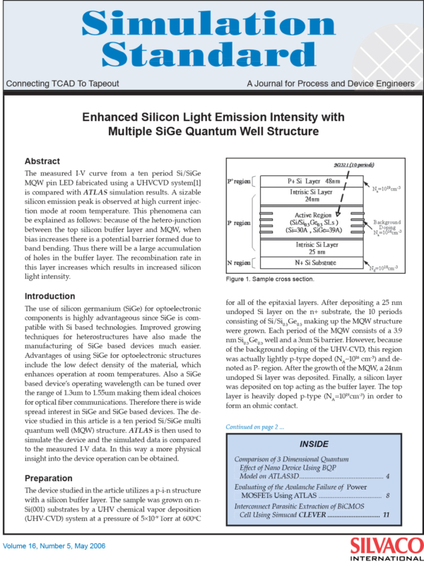
The measured I-V curve from a ten period Si/SiGe MQW pin LED fabricated using a UHVCVD system is compared with ATLAS simulation results. A sizable silicon emission peak is observed at high current injection mode at room temperature. This phenomena can be explained as follows: because of the hetero-junction between the top silicon buffer layer and MQW, when bias increases there is a potential barrier formed due to band bending. Thus there will be a large accumulation of holes in the buffer layer. The recombination rate in this layer increases which results in increased silicon light intensity.
Introduction
The use of silicon germanium (SiGe) for optoelectronic components is highly advantageous since SiGe is compatible with Si based technologies. Improved growing techniques for heterostructures have also made the manufacturing of SiGe based devices much easier. Advantages of using SiGe for optoelectronic structures include the low defect density of the material, which enhances operation at room temperatures. Also a SiGe based device’s operating wavelength can be tuned over the range of 1.3um to 1.55um making them ideal choices for optical fiber communications. Therefore there is wide spread interest in SiGe and SiGe based devices. The device studied in this article is a ten period Si/SiGe multi quantum well (MQW) structure. ATLAS is then used to simulate the device and the simulated data is compared to the measured I-V data. In this way a more physical insight into the device operation can be obtained.
Preparation
The device studied in the article utilizes a p-i-n structure with a silicon buffer layer. The sample was grown on n-Si(001) substrates by a UHV chemical vapor deposition (UHV-CVD) system at a pressure of 510-9 Torr at 600oC for all of the epitaxial layers. After depositing a 25 nm undoped Si layer on the n+ substrate, the 10 periods consisting of Si/Si0.5Ge0.5 making up the MQW structure were grown. Each period of the MQW consists of a 3.9 nm Si0.5Ge0.5 well and a 3nm Si barrier. However, because of the background doping of the UHV-CVD, this region was actually lightly p-type doped (NA~1016 cm-3) and denoted as P- region. After the growth of the MQW, a 24nm undoped Si layer was deposited. Finally, a silicon layer was deposited on top acting as the buffer layer. The top layer is heavily doped p-type (NA=1019cm-3) in order to form an ohmic contact.


