Crosstalk Between Pixels of Organic Photo-Voltaic Devices
Introduction
For various technological reasons, LEDs and as well as photo-voltaic devices frequently use PEDOT:PSS on top of ITO contacts as a hole injecting or hole collecting layer, respectively. However, due to the presence of this layer, a direct parasitic current path opens up between the ITO contacts of neighboring pixels.
Next to its influence on the optical properties of the layered device, the presence of the PEDOT:PSS layer between pixels may modify the potential profile in the active organic layer underneath and may therefore influence the lateral charge separation process in the illuminated device, causing optical induced electric crosstalk.
In this Simulation Standard we demonstrate the principal capabilities needed to simulate crosstalk between neighboring illuminated and dark pixels.
Device and Models
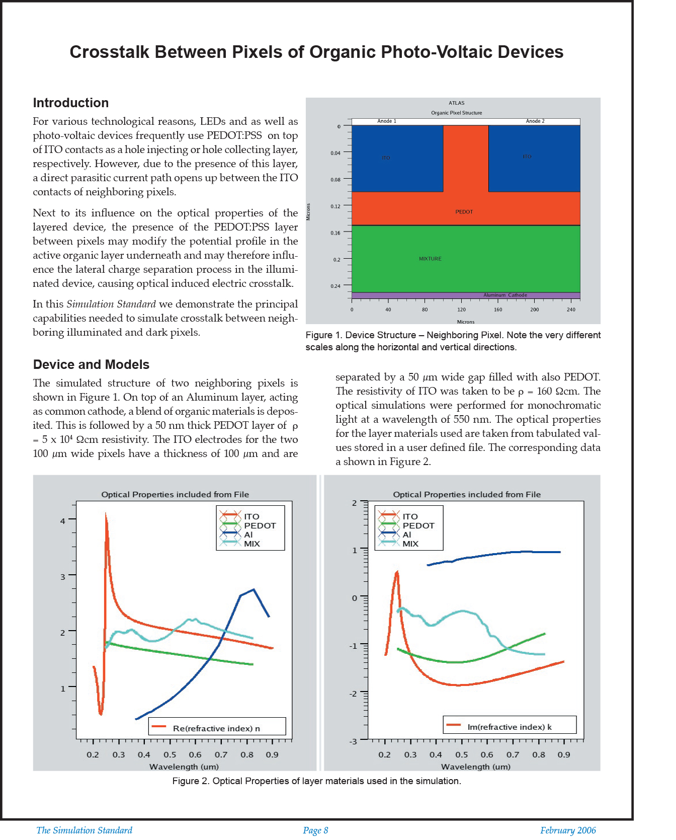
The simulated structure of two neighboring pixels is shown in Figure 1. On top of an Aluminum layer, acting as common cathode, a blend of organic materials is deposited. This is followed by a 50 nm thick PEDOT layer of ![]() = 5 x 104
= 5 x 10⁴ ![]() cm resistivity. The ITO electrodes for the two 100 µm wide pixels have a thickness of 100 µm and are separated by a 50 µm wide gap filled with also PEDOT. The resistivity of ITO was taken to be
cm resistivity. The ITO electrodes for the two 100 µm wide pixels have a thickness of 100 µm and are separated by a 50 µm wide gap filled with also PEDOT. The resistivity of ITO was taken to be ![]() = 160
= 160 ![]() cm. The optical simulations were performed for monochromatic light at a wavelength of 550 nm. The optical properties for the layer materials used are taken from tabulated values stored in a user defined file. The corresponding data a shown in Figure 2.
cm. The optical simulations were performed for monochromatic light at a wavelength of 550 nm. The optical properties for the layer materials used are taken from tabulated values stored in a user defined file. The corresponding data a shown in Figure 2.


