Atlas Device Simulation of Amorphous Oxide Semiconductor Thin-Film Transistors
1. Introduction
Amorphous oxide semiconductor materials have attracted much attention as key components of TFTs for flexible electronics [1]. The advantages of such materials include flexibility and transparency which are compatible with plastic substrates, and higher mobilities than those of amorphous-Si and organic semiconductor TFT materials.
In this paper, the operation of an amorphous oxide semiconductor TFT was analyzed by the two-dimensional numerical simulator ATLAS to verify the applicability of standard drift-diffusion models to an amorphous oxide semiconductor material.
2. The Device Structure and Models
An amorphous oxide semiconductor TFT fabricated and reported by Nomura et al. [2] was simulated and resultant ID-VD and ID-VG curves were compared with measured data.
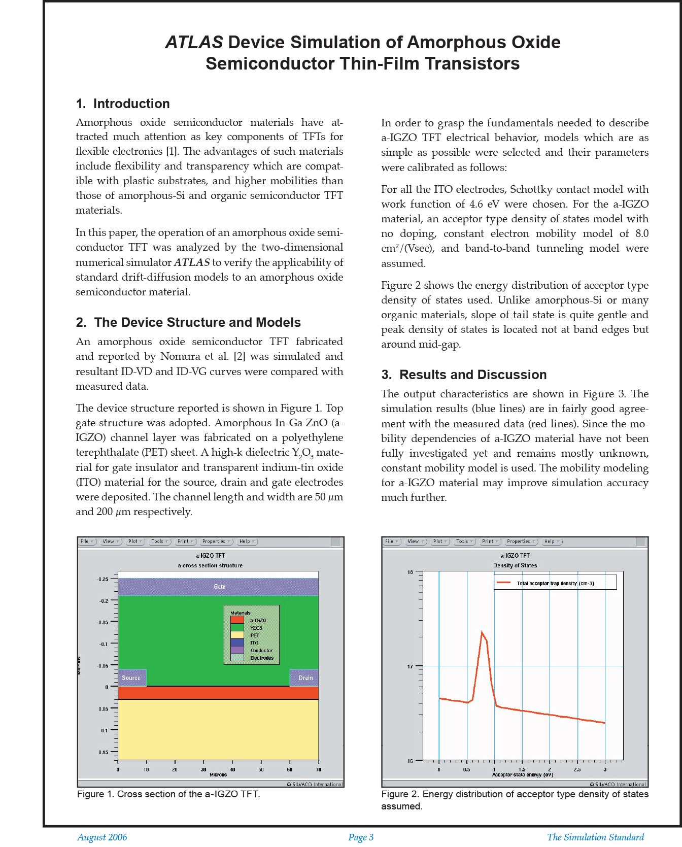
The device structure reported is shown in Figure 1. Top gate structure was adopted. Amorphous In-Ga-ZnO (a-IGZO) channel layer was fabricated on a polyethylene terephthalate (PET) sheet. A high-k dielectric Y2O3 material for gate insulator and transparent indium-tin oxide (ITO) material for the source, drain and gate electrodes were deposited. The channel length and width are 50 µm and 200 µm respectively.
In order to grasp the fundamentals needed to describe a-IGZO TFT electrical behavior, models which are as simple as possible were selected and their parameters were calibrated as follows:
For all the ITO electrodes, Schottky contact model with work function of 4.6 eV were chosen. For the a-IGZO material, an acceptor type density of states model with no doping, constant electron mobility model of 8.0 cm2/(Vsec), and band-to-band tunneling model were assumed.
Figure 2 shows the energy distribution of acceptor type density of states used. Unlike amorphous-Si or many organic materials, slope of tail state is quite gentle and peak density of states is located not at band edges but around mid-gap.


