Athena/Optolith Simulation of Proximity Lithography
1. Introduction
Photolithography simulation is a very important part of TCAD. Accurate and predictive lithography simulation saves time and money spent on development and calibration of semiconductor technology processes. Photolithography simulation has also become a critical element of modern design for manufacturability (DFM) flows. Most lithography simulators are focused on resolution enhancement for projection imaging. This “standard” lithography technology is getting more expensive for each subsequent technology node. The proximity printing (i.e. imaging without reduction lens) is obviously more cost effective in printing relatively big features on micron scale. This method is effectively used in many applications, e.g. power device and flat panel display manufacturing. This paper briefly discusses implementation and use of proximity printing module in ATHENA/Optolith.
2. Proximity Lithography
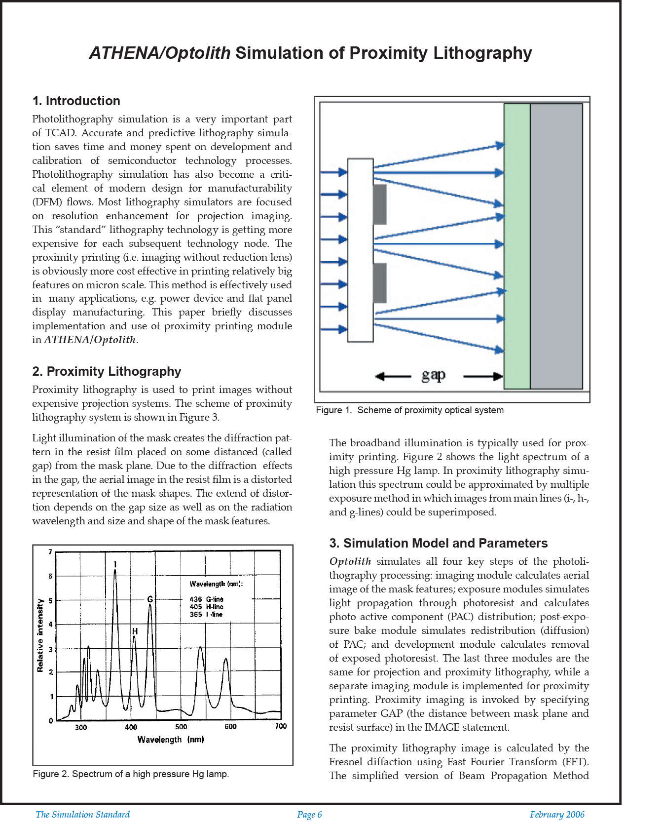
Proximity lithography is used to print images without expensive projection systems. The scheme of proximity lithography system is shown in Figure 3.
Light illumination of the mask creates the diffraction pattern in the resist film placed on some distanced (called gap) from the mask plane. Due to the diffraction effects in the gap, the aerial image in the resist film is a distorted representation of the mask shapes. The extend of distortion depends on the gap size as well as on the radiation wavelength and size and shape of the mask features.
The broadband illumination is typically used for proximity printing. Figure 2 shows the light spectrum of a high pressure Hg lamp. In proximity lithography simulation this spectrum could be approximated by multiple exposure method in which images from main lines (i-, h-, and g-lines) could be superimposed.


