Comparison of 3-Dimensional Quantum Effects in Nano Devices Using the ATLAS 3D BQP Model
Introduction
With the MOSFET gate lengths scaling down to sub-20nms many kinds of devices have been proposed and researched such as double-gate, tri-gate, four-gate and gate-all-around (wire) MOSFETs.
In this work, the carrier distribution and capacitance of these 4-types of nano MOSFET were compared using the Bohm Quantum Potential Model [1] in ATLAS3D.
Nanodevice : Geometry and Structure
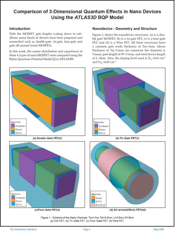
Figure 1, shows the nanodevice structures. (a) is a double-gate MOSFET, (b) is a tri-gate FET, (c) is a four-gate FET, and (d) is a Wire FET. All these structures have a common gate oxide thickness of Tox=1nm, silicon thickness of Tsi=5.6nm (on nanowire the diameter is 5.6nm), gate length of W=5.6nm, and total device length of L=8nm. Also, the doping level used is NA=1e16 cm-3 and ND=1e20 cm-3.
Simulation
The Bohm Quantum Potential (BQP) model is an expansion of the Wigner equation and calculates the effects of quantum confinement on the electron and hole concentration and C-V curves [1].
As we have 4 different structures, we compared carrier concentration on the center cutplane of the gate as shown in Figure 2.


