Simulation Standard
Silvaco面向半导体工艺和器件仿真工程师推出的技术刊物
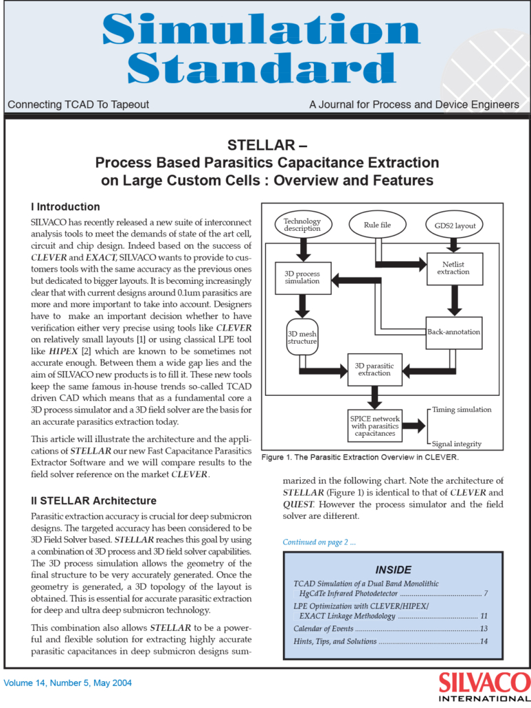
STELLAR – Process Based Parasitics Capacitance Extraction on Large Custom Cells
SILVACO has recently released a new suite of interconnect analysis tools to meet the demands of state of the art cell, circuit and chip design.
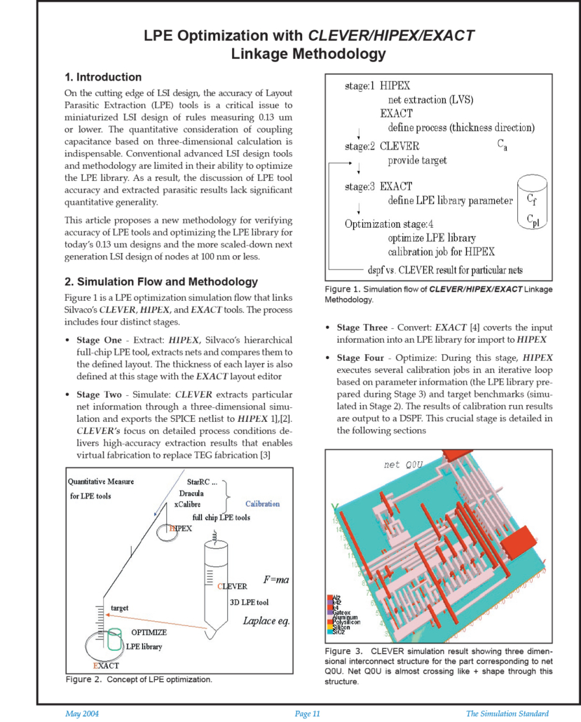
LPE Optimization with Clever/Hipex/Exact Linkage Methodology
On the cutting edge of LSI design, the accuracy of Layout Parasitic Extraction (LPE) tools is a critical issue to miniaturized LSI design of rules measuring 0.13 um or lower. The quantitative consideration of coupling capacitance based on three-dimensional calculation is indispensable. Conventional advanced LSI design tools and methodology are limited in their ability to optimize the LPE library. As a result, the discussion of LPE tool accuracy and extracted parasitic results lack significant quantitative generality.
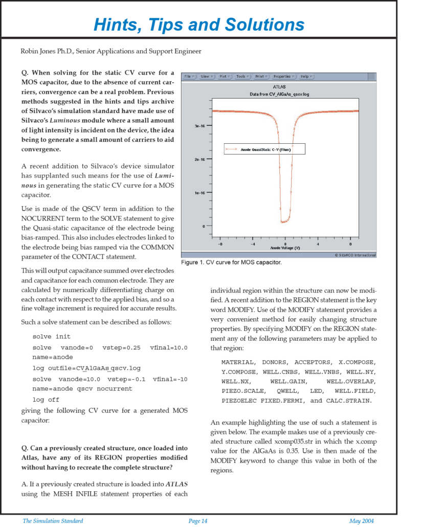
When solving for the static CV curve for a MOS capacitor, due to the absence of current carriers
When solving for the static CV curve for a MOS capacitor, due to the absence of current carriers, convergence can be a real problem. Previous methods suggested in the hints and tips archive of Silvaco’s simulation standard have made use of Silvaco’s Luminous module where a small amount of light intensity is incident on the device, the idea being to generate a small amount of carriers to aid convergence.
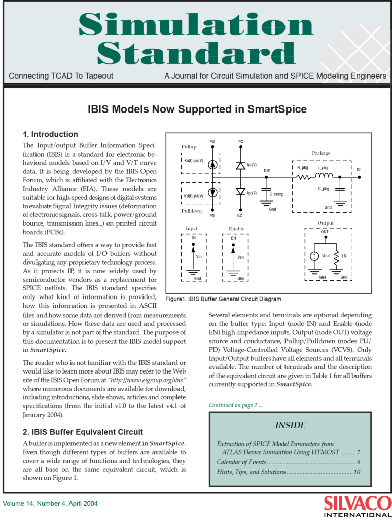
IBIS Models Now Supported in SmartSpice
Expert Parametric Wire (Pwire) is a complex group of objects containing, a single wire named master wire, any number of subparts such as enclosure wires, offset wires and sets of rectangles. Pwire objects enable extremely quick and efficient creation and editing of guard rings and shielded paths which are increasingly important due to higher integration density of IC designs.
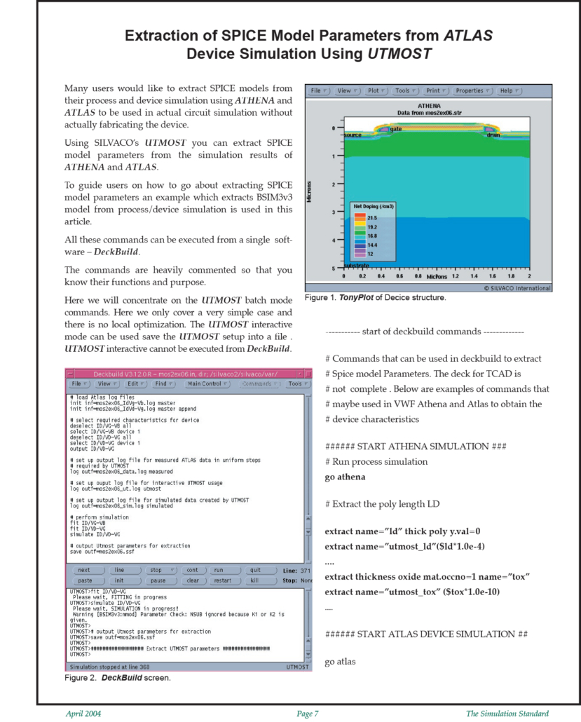
Extraction of SPICE Model Parameters from Atlas Device Simulation Using Utmost
Many users would like to extract SPICE models from their process and device simulation using Athena and Atlas to be used in actual circuit simulation without actually fabricating the device.
Using SILVACO's Utmost you can extract SPICE model parameters from the simulation results of Athena and Atlas.
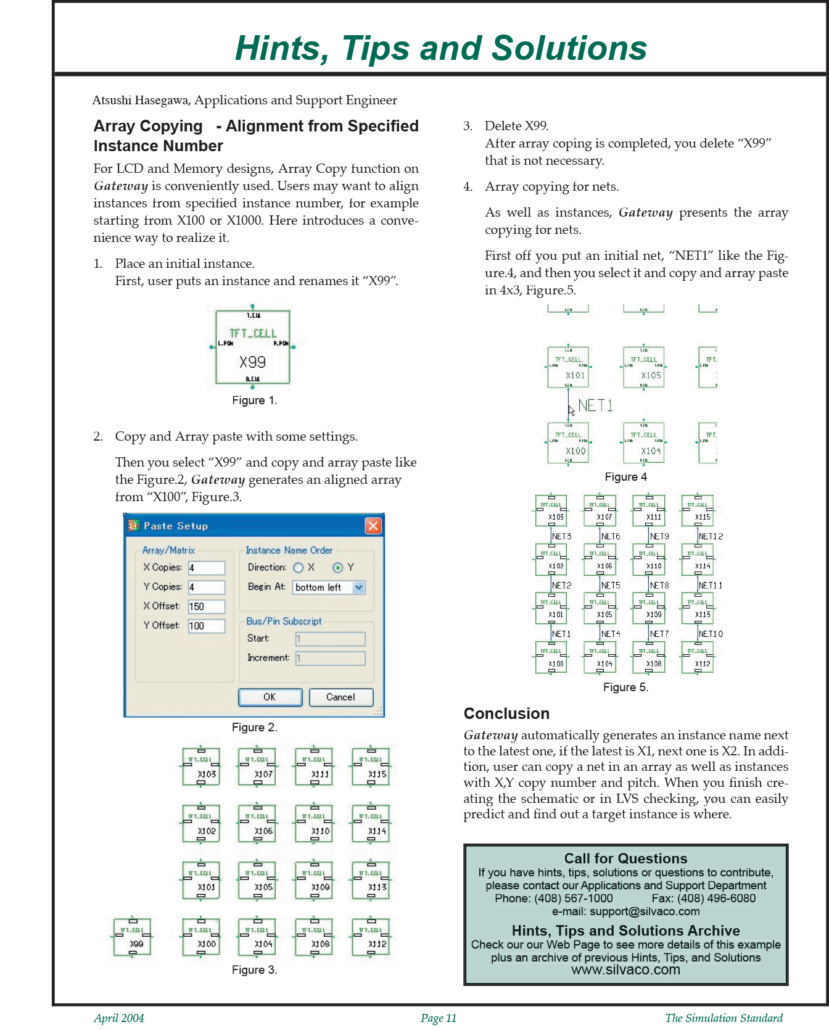
Array Copying – Alignment from Specified Instance Number
For LCD and Memory designs, Array Copy function on Gateway is conveniently used. Users may want to align instances from specified instance number, for example starting from X100 or X1000. Here introduces a convenience way to realize it.

