
Simulation Standard
Silvaco面向半导体工艺和器件仿真工程师推出的技术刊物
 https://silvaco.com/wp-content/uploads/2020/03/simstd_Q3_2012_a1.jpg
1012
782
Ingrid Schwarz
/wp-content/uploads/2019/11/silvaco-logo.png
Ingrid Schwarz2012-07-01 18:23:022021-10-13 10:22:54Actuation Voltage For a Cantilever Switch in MEMS
https://silvaco.com/wp-content/uploads/2020/03/simstd_Q3_2012_a1.jpg
1012
782
Ingrid Schwarz
/wp-content/uploads/2019/11/silvaco-logo.png
Ingrid Schwarz2012-07-01 18:23:022021-10-13 10:22:54Actuation Voltage For a Cantilever Switch in MEMS https://silvaco.com/wp-content/uploads/2020/03/simstd_Q2_2012_a4.jpg
1012
782
Ingrid Schwarz
/wp-content/uploads/2019/11/silvaco-logo.png
Ingrid Schwarz2012-04-01 18:18:362021-10-13 10:22:54Current Collapse Phenomenon in GaN HFETs resulting from Intentional Bulk Iron (Fe) Doping and Un-intentional Interface Traps
https://silvaco.com/wp-content/uploads/2020/03/simstd_Q2_2012_a4.jpg
1012
782
Ingrid Schwarz
/wp-content/uploads/2019/11/silvaco-logo.png
Ingrid Schwarz2012-04-01 18:18:362021-10-13 10:22:54Current Collapse Phenomenon in GaN HFETs resulting from Intentional Bulk Iron (Fe) Doping and Un-intentional Interface Traps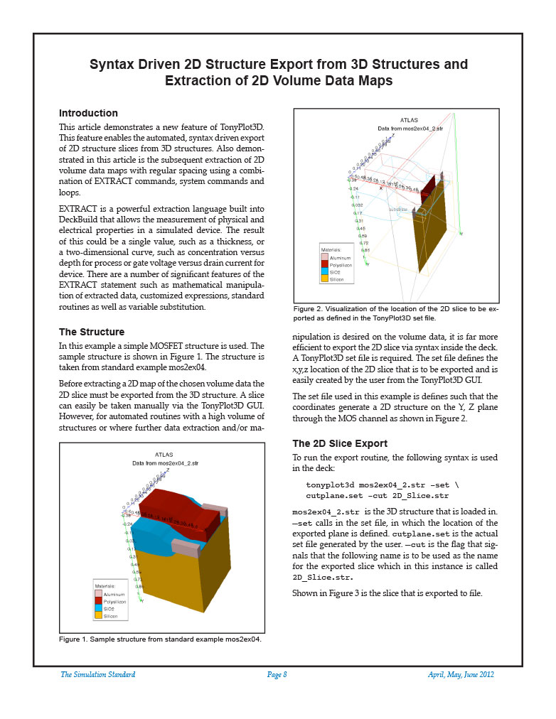 https://silvaco.com/wp-content/uploads/2020/03/simstd_Q2_2012_a3.jpg
1012
782
Ingrid Schwarz
/wp-content/uploads/2019/11/silvaco-logo.png
Ingrid Schwarz2012-04-01 18:15:272021-10-13 10:23:46Syntax Driven 2D Structure Export from 3D Structures and Extraction of 2D Volume Data Maps
https://silvaco.com/wp-content/uploads/2020/03/simstd_Q2_2012_a3.jpg
1012
782
Ingrid Schwarz
/wp-content/uploads/2019/11/silvaco-logo.png
Ingrid Schwarz2012-04-01 18:15:272021-10-13 10:23:46Syntax Driven 2D Structure Export from 3D Structures and Extraction of 2D Volume Data Maps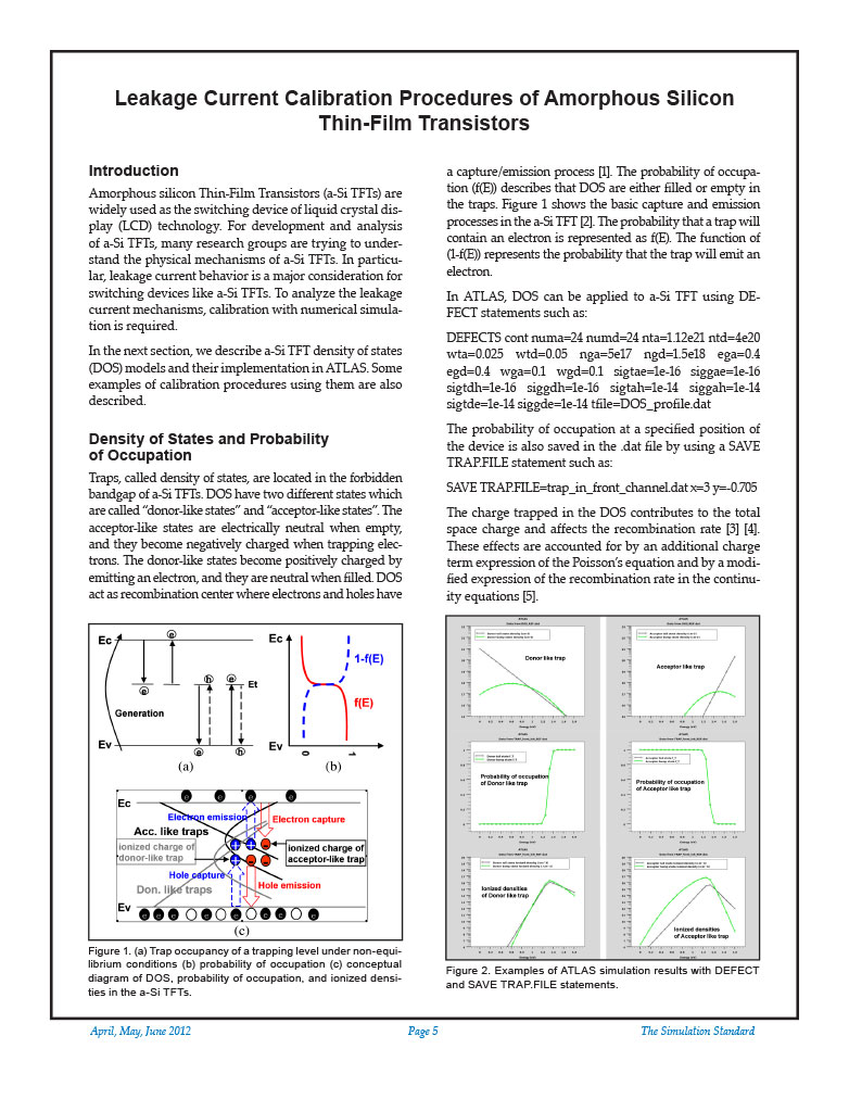 https://silvaco.com/wp-content/uploads/2020/03/simstd_Q2_2012_a2.jpg
1012
782
Ingrid Schwarz
/wp-content/uploads/2019/11/silvaco-logo.png
Ingrid Schwarz2012-04-01 18:07:172021-10-13 10:23:46Leakage Current Calibration Procedures of Amorphous Silicon Thin-Film Transistors
https://silvaco.com/wp-content/uploads/2020/03/simstd_Q2_2012_a2.jpg
1012
782
Ingrid Schwarz
/wp-content/uploads/2019/11/silvaco-logo.png
Ingrid Schwarz2012-04-01 18:07:172021-10-13 10:23:46Leakage Current Calibration Procedures of Amorphous Silicon Thin-Film Transistors https://silvaco.com/wp-content/uploads/2020/03/simstd_Q2_2012_a1.jpg
1012
782
Ingrid Schwarz
/wp-content/uploads/2019/11/silvaco-logo.png
Ingrid Schwarz2012-04-01 17:58:352021-10-13 10:23:463D TFT Simulation
https://silvaco.com/wp-content/uploads/2020/03/simstd_Q2_2012_a1.jpg
1012
782
Ingrid Schwarz
/wp-content/uploads/2019/11/silvaco-logo.png
Ingrid Schwarz2012-04-01 17:58:352021-10-13 10:23:463D TFT Simulation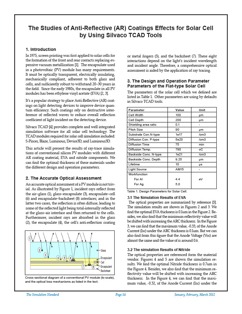 https://silvaco.com/wp-content/uploads/2020/03/simstd_Q1_2012_a5.jpg
1012
782
Ingrid Schwarz
/wp-content/uploads/2019/11/silvaco-logo.png
Ingrid Schwarz2012-01-01 17:46:312021-10-13 10:23:47The Studies of Anti-Reflective (AR) Coatings Effects for Solar Cell by Using Silvaco TCAD Tools
https://silvaco.com/wp-content/uploads/2020/03/simstd_Q1_2012_a5.jpg
1012
782
Ingrid Schwarz
/wp-content/uploads/2019/11/silvaco-logo.png
Ingrid Schwarz2012-01-01 17:46:312021-10-13 10:23:47The Studies of Anti-Reflective (AR) Coatings Effects for Solar Cell by Using Silvaco TCAD Tools