Simulation Standard
Silvaco面向半导体工艺和器件仿真工程师推出的技术刊物
State of the Art 2D and 3D Process and Device Simulation of GaN-Based Devices
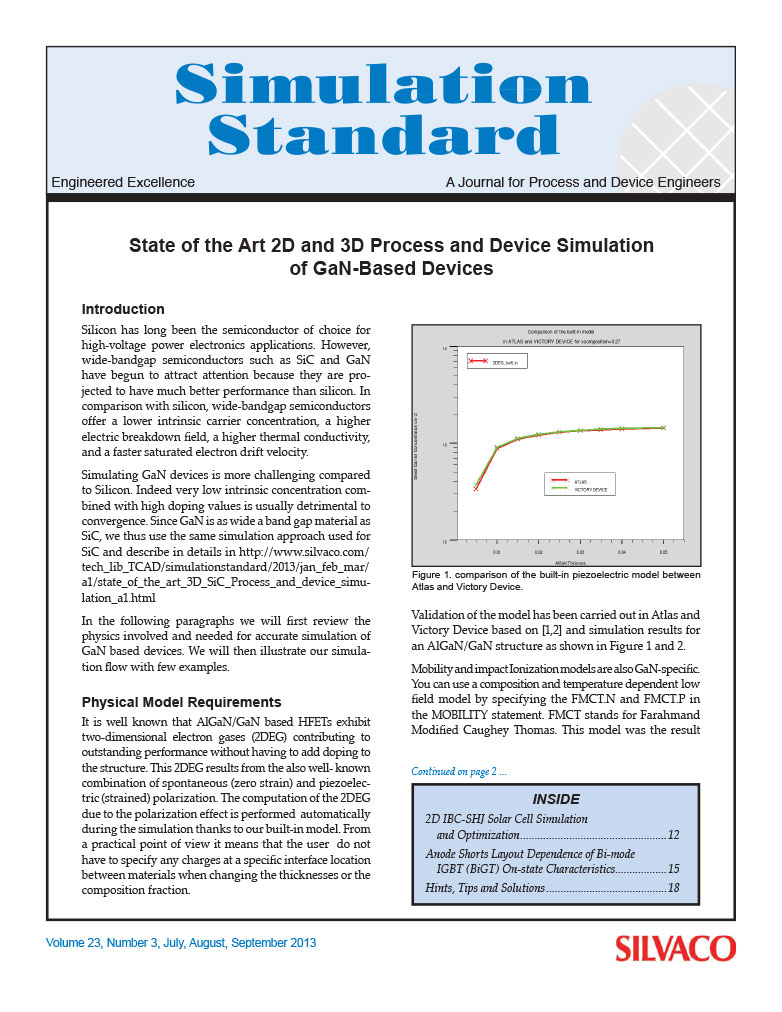
Silicon has long been the semiconductor of choice for high-voltage power electronics applications. However, wide-bandgap semiconductors such as SiC and GaN have begun to attract attention because they are projected to have much better performance than silicon. In comparison with silicon, wide-bandgap semiconductors offer a lower intrinsic carrier concentration, a higher electric breakdown field, a higher thermal conductivity, and a faster saturated electron drift velocity.
Hints, Tips and Solutions – Setup Athena Monte Carlo Simulation of Ion Implantation in Silicon Carbide
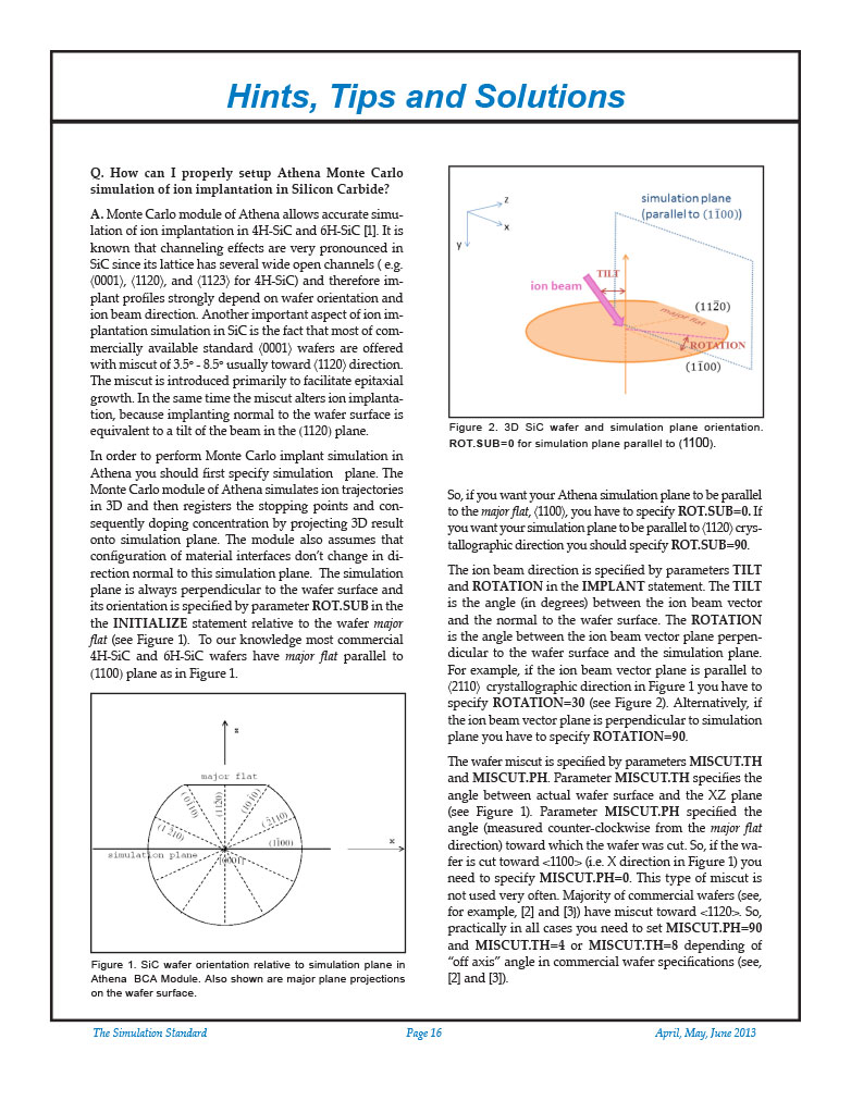
Monte Carlo module of Athena allows accurate simulation of ion implantation in 4H-SiC and 6H-SiC [1]. It is known that channeling effects are very pronounced in SiC since its lattice has several wide open channels ( e.g. 〈0001〉, 〈1120〉, and 〈1123〉 for 4H-SiC) and therefore implant profiles strongly depend on wafer orientation and ion beam direction. Another important aspect of ion implantation simulation in SiC is the fact that most of commercially available standard 〈0001〉 wafers are offered with miscut of 3.5° - 8.5° usually toward 〈1120〉 direction. The miscut is introduced primarily to facilitate epitaxial growth. In the same time the miscut alters ion implantation, because implanting normal to the wafer surface is equivalent to a tilt of the beam in the (1120) plane.
TCAD Simulation of Multiple Quantum Well Infrared Photodetector (QWIP)
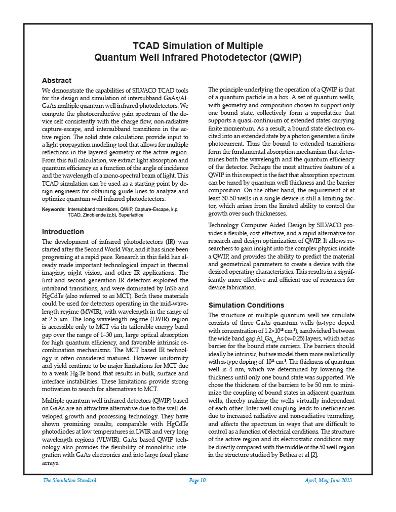
We demonstrate the capabilities of SILVACO TCAD tools for the design and simulation of intersubband GaAs/AlGaAs multiple quantum well infrared photodetectors. We compute the photoconductive gain spectrum of the device self consistently with the charge flow, non-radiative capture-escape, and intersubband transitions in the active region. The solid state calculations provide input to a light propagation modeling tool that allows for multiple reflections in the layered geometry of the active region. From this full calculation, we extract light absorption and quantum efficiency as a function of the angle of incidence and the wavelength of a mono-spectral beam of light. This TCAD simulation can be used as a starting point by design engineers for obtaining guide lines to analyze and optimize quantum well infrared photodetectors.
The Extended Gaussian Disorder Model in Atlas
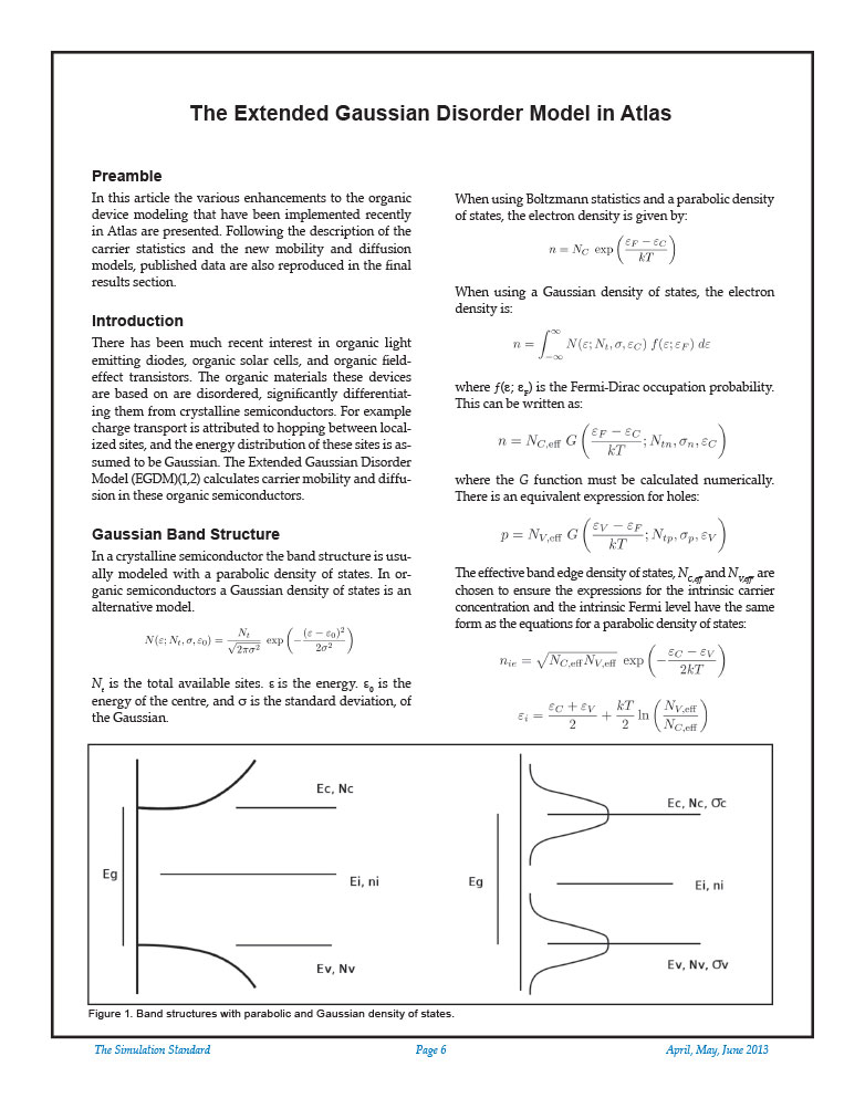
In this article the various enhancements to the organic device modeling that have been implemented recently in Atlas are presented. Following the description of the carrier statistics and the new mobility and diffusion models, published data are also reproduced in the final results section.
Simulation of Ion Beam Etching of Patterned Nanometer-scale Magnetic Structures for High-Density Storage Applications
Fabrication of various nano-structures often requires mask controlled or patterned etching of materials. The chemical or wet etch methods cannot be used for nanoscale geometries due to the substantial isotropic component of etch rate. Therefore, various plasma or reactive ion etching method are typically used. Unfortunately, some materials do not easily form volatile reaction products and all types of chemically assist etching becomes problematic. Among those materials are elements such as Co, Ni, Fe, Pt, and Cr which are usually used in magnetic nano-structure technologies. Therefore, ion beam etching or ion milling is the most suitable method to pattern these materials [1].
State of the Art 3D SiC Process and Device Simulation
Silicon has long been the semiconductor of choice for high-voltage power electronics applications [1,2]. However, wide-bandgap semiconductors such as SiC have begun to attract attention because they are projected to have much better performance than silicon [3-7]. In comparison with silicon, wide-bandgap semiconductors offer a lower intrinsic carrier concentration (10 to 35 orders of magnitude), a higher electric breakdown field (4 to 20 times), a higher thermal conductivity (3 to 13 times), and a faster saturated electron drift velocity (2 to 2.5 times).

