Simulation Standard
Silvaco面向半导体工艺和器件仿真工程师推出的技术刊物
Hints, Tips, and Solutions – Simulate Rapid Thermal Annealing Temperature Transients in Vacuum
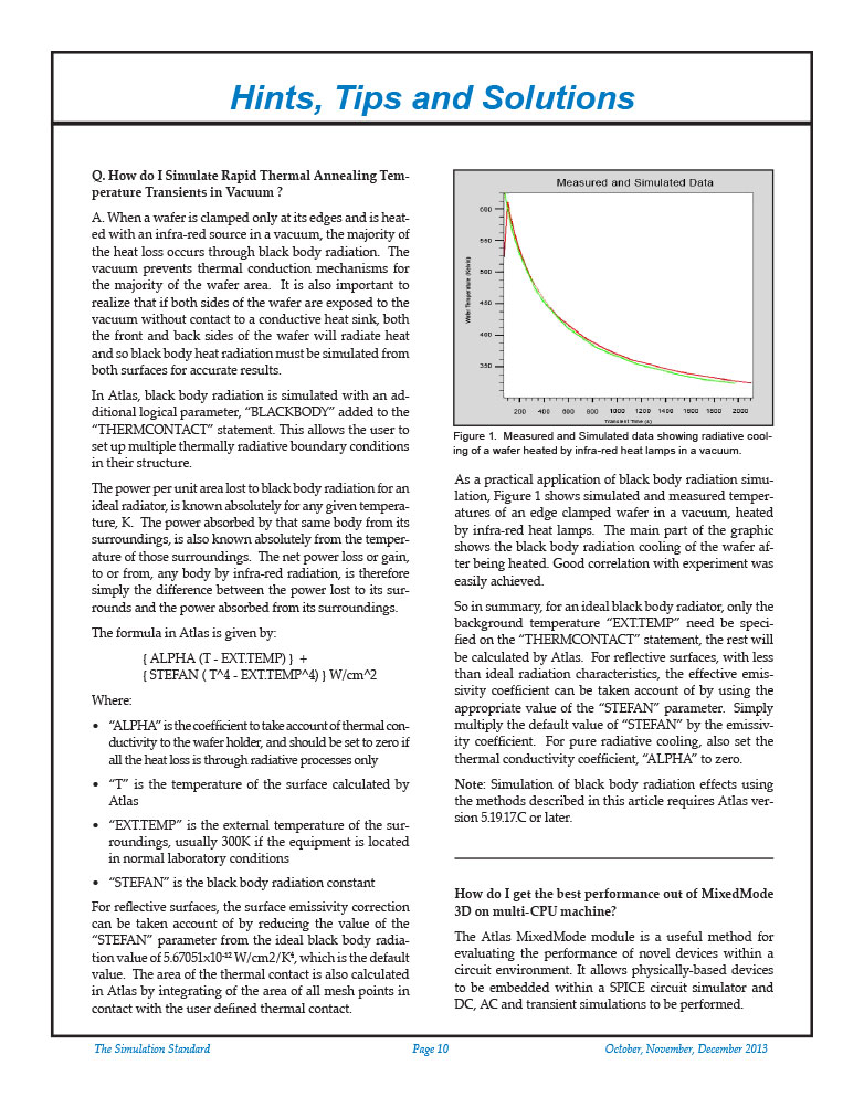
When a wafer is clamped only at its edges and is heated with an infra-red source in a vacuum, the majority of the heat loss occurs through black body radiation. The vacuum prevents thermal conduction mechanisms for the majority of the wafer area. It is also important to realize that if both sides of the wafer are exposed to the vacuum without contact to a conductive heat sink, both the front and back sides of the wafer will radiate heat and so black body heat radiation must be simulated from both surfaces for accurate results.
Atlas Simulation of a Wide Bandgap Gallium Oxide (Ga2O3) MOSFET
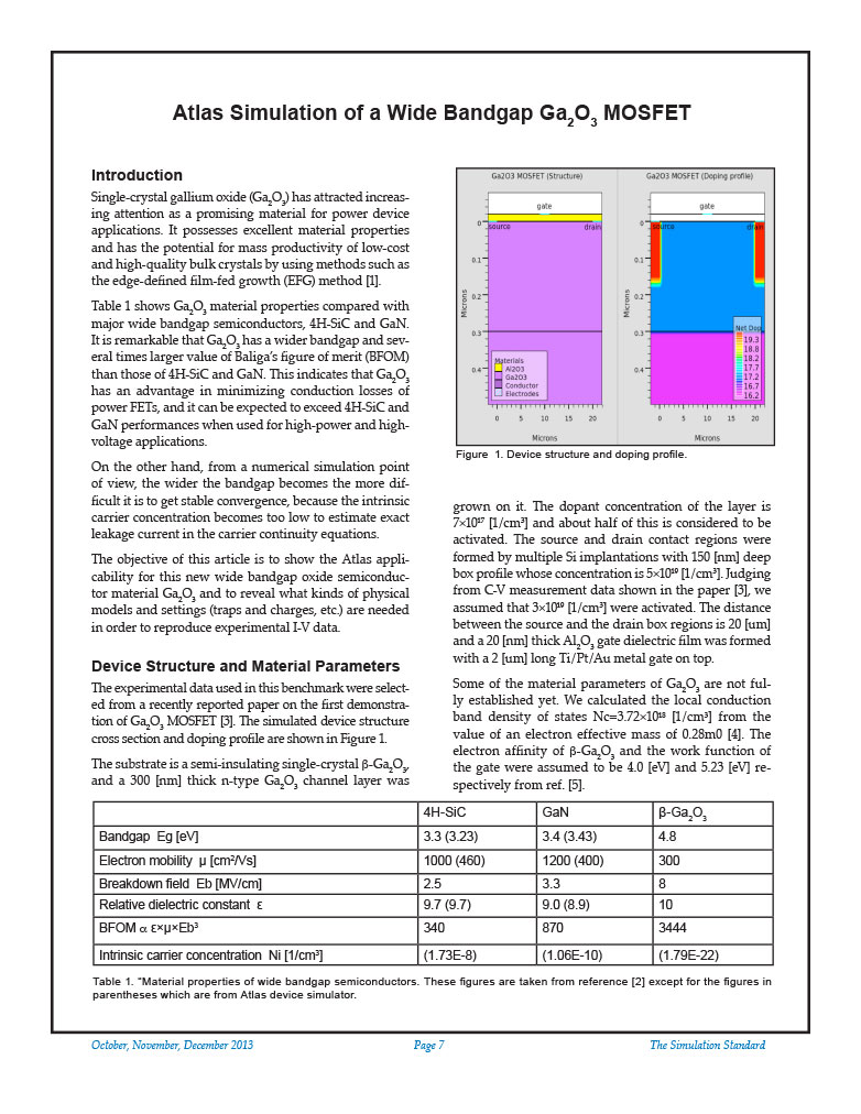
Single-crystal gallium oxide (Ga2O3) has attracted increasing attention as a promising material for power device applications. It possesses excellent material properties and has the potential for mass productivity of low-cost and high-quality bulk crystals by using methods such as the edge-defined film-fed growth (EFG) method [1].
Simulation of a DBR Edge Emitting Laser with External Air Gap Tuning Mirror
A methodology for simulating an edge emitting laser is demonstrated that incorporates a distributed Bragg Reflector (DBR) as one of the mirrors, with the other being a variable air gap external planar mirror that is used as a method for fine tuning the lasing wavelength. This type of calculation requires non uniformity of the dielectric’s static and dynamic (pumping) properties in both the transverse and longitudinal directions, together with self consistent coupling to the external tuning cavity. A key challenge addressed is the proper treatment of the open nature of the cavity, such that the amplitudes of the outgoing waves leaving the facets are consistent with the cavity interior and facet reflectivity. Mode competition and hopping are natural consequences of the methodology developed. In the model developed here, the spatial hole burning effects, cross and self-saturation effects can be included while accounting for the degree of spatial overlap of modes. We also account for diffraction losses at the output facet which can become important in the case of strong index guiding.
Anode Shorts Layout Dependence of Bi-mode IGBT (BiGT) On-state Characteristics
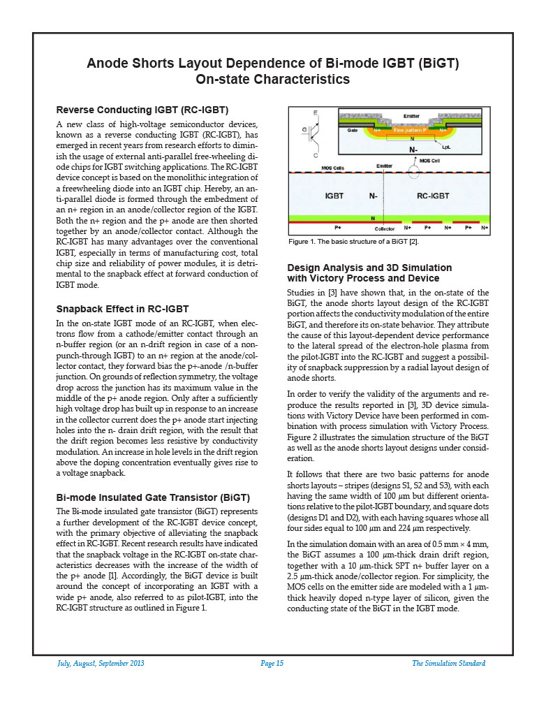
A new class of high-voltage semiconductor devices, known as a reverse conducting IGBT (RC-IGBT), has emerged in recent years from research efforts to diminish the usage of external anti-parallel free-wheeling diode chips for IGBT switching applications. The RC-IGBT device concept is based on the monolithic integration of a freewheeling diode into an IGBT chip. Hereby, an anti-parallel diode is formed through the embedment of an n+ region in an anode/collector region of the IGBT. Both the n+ region and the p+ anode are then shorted together by an anode/collector contact. Although the RC-IGBT has many advantages over the conventional IGBT, especially in terms of manufacturing cost, total chip size and reliability of power modules, it is detrimental to the snapback effect at forward conduction of IGBT mode.
Hints, Tips and Solutions – Compare the Results of Breakdown Simulations with Hatakeyama’s Impact Ionization Model for 4H-SiC Based Power Devices
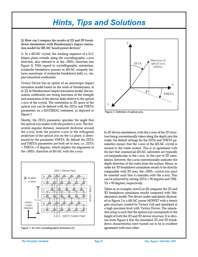
In a 4H-SiC crystal, the stacking sequence of a Si-C bilayer plane extends along the crystallographic c-axis direction, also referred to as the <0001> direction (see Figure 1). With regard to crystallographic orientation, avalanche breakdown process in 4H-SiC uniquely features anisotropy of avalanche breakdown field, i.e., impact ionization coefficients.
2D IBC-SHJ Solar Cell Simulation and Optimization
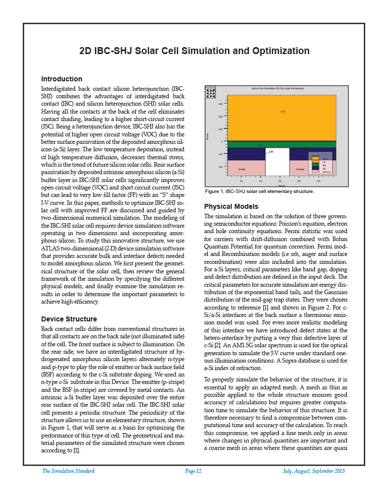
Interdigitated back contact silicon heterojunction (IBC-SHJ) combines the advantages of interdigitated back contact (IBC) and silicon heterojunction (SHJ) solar cells. Having all the contacts at the back of the cell eliminates contact shading, leading to a higher short-circuit current (JSC). Being a heterojunction device, IBC-SHJ also has the potential of higher open circuit voltage (VOC) due to the better surface passivation of the deposited amorphous silicon (a-Si) layer. The low temperature deposition, instead of high temperature diffusion, decreases thermal stress, which is the trend of future silicon solar cells. Rear surface passivation by deposited intrinsic amorphous silicon (a-Si) buffer layer in IBC-SHJ solar cells significantly improves open circuit voltage (VOC) and short circuit current (JSC) but can lead to very low fill factor (FF) with an “S” shape J-V curve. In this paper, methods to optimize IBC-SHJ solar cell with improved FF are discussed and guided by two-dimensional numerical simulation. The modeling of the IBC-SHJ solar cell requires device simulation software operating in two dimensions and incorporating amorphous silicon. To study this innovative structure, we use ATLAS two-dimensional (2-D) device simulation software that provides accurate bulk and interface defects needed to model amorphous silicon. We first present the geometrical structure of the solar cell, then review the general framework of the simulation by specifying the different physical models, and finally examine the simulation results in order to determine the important parameters to achieve high efficiency.

