Simulation Standard
Silvaco面向半导体工艺和器件仿真工程师推出的技术刊物
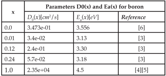
An Empirical Composition Dependent Model of Dopant Diffusion Coefficients in Si, Si1-x Gex and Ge Material Systems
Previously published fast empirical models for diffusion coefficients in silicon-germanium (Si1-x Gex) [1][2] were not applicable to high germanium content x≥0.5 and hence did not properly extend towards germanium. For some dopants, diffusion coefficients become very small and hence this model cannot be applied to devices containing silicon-germanium with high germanium content or devices containing silicon, silicon-germanium and germanium
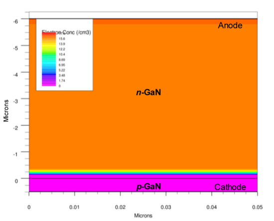
TCAD Simulation of Leakage Through Threading Dislocations in GaN-based pn-diodes
Gallium nitride (GaN)-based devices for power electronics show superior performance in comparison to silicon carbide and silicon-based devices [1]–[3]. The development of vertical devices, like pn-diodes and power HEMTs results in higher power density and voltage handling. One of the key parameters of this technology is the dislocation density. This is lower in free-standing GaN-on-GaN epitaxy than in heteroepitaxial GaN growth on different substrates like SiC or Si, but still has a density of 104-106 cm-2 [4]. The diode reverse leakage seems to be related to the dislocation density, and it can be modelled with a Poole-Frenkel or a hopping conduction mechanism [5]. The Poole-Frenkel model is already implemented in the trap-assisted tunnelling model in Silvaco Atlas [6]. For the leakage in threading dislocations a variable-range hopping (VRH) model has been implemented in the simulator, based on Ref. [7].
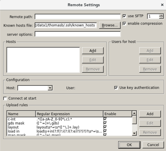
Hints, Tips and Solutions – DeckBuild Remote VM Setup
This document describes how to setup a virtual environment suitable for the deckbuild remote mode.
The host system to consider shall be Windows (7 or 10). The goal is to use the windows version of the TCAD GUI tools TonyPlot and DeckBuild and to run any simulation (Victory, Athena, Clever) on a Linux Virtual Machine (VM).
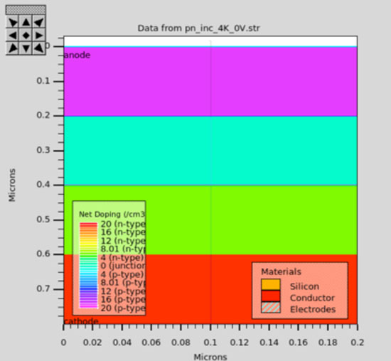
TCAD Simulation of Si and GaAs p-n Junction Devices at Cryogenic Temperatures, Down to 2 K
Cryogenic electronics plays a fundamental role in several applications, such as spacecraft, high-energy physics experiments, metrology, superconductive astronomical detectors and, with the increased interest in quantum computing, the manipulation of quantum bits (qubits) [1]. Outstanding characteristics have been reported for advanced CMOS technologies operating at cryogenic temperature in terms of on-state current, leakage current, subthreshold swing, and transconductance [2]. This represents an excellent opportunity to use such advanced technologies to design and implement a quantum computing control system (including multiplexers, LNAs, and RF oscillators) and introduce it inside the refrigerator together with the qubits [3]. Another recently growing field of application is the cryogenic silicon photonics [4].
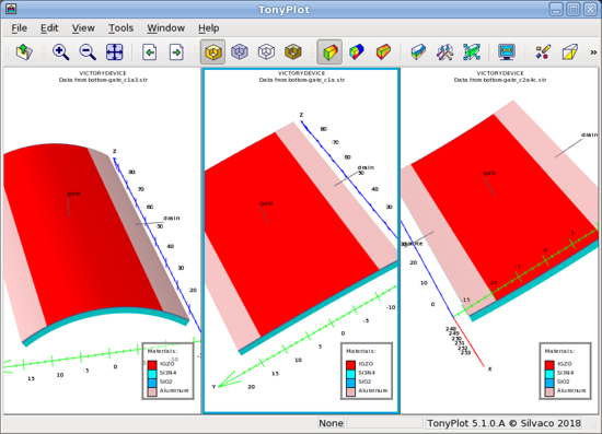
Bi-axial Deformation with Victory Mesh for Flexible Electronic Applications
For high performance large area flexible electronics, amorphous metal oxide semiconductor based thin film transistors offer many advantages. These include high mobility, steep sub-threshold and ultralow leakage current, with low cost and large area manufacturability.
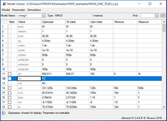
TCAD-based GaN HEMT Scalable Modeling Flow Using the MVSG Compact Model
Gallium Nitride High Electron Mobility (GaN HEMT) device technology has gained a lot of traction during the last years. These devices have significant advantages compared to Silicon in user applications such as high frequency/high power amplifiers, radar systems, power conversion and applications where stability over a wide range of temperatures is required, such as automotive-related.

