Simulation Standard
Silvaco面向半导体工艺和器件仿真工程师推出的技术刊物
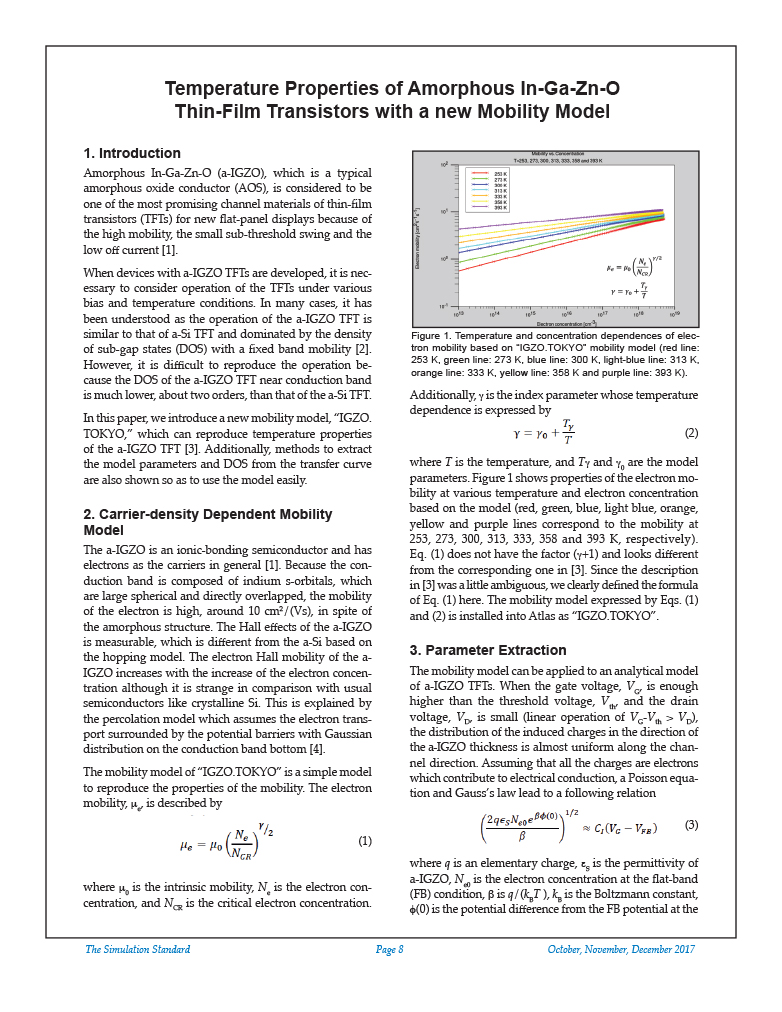
Temperature Properties of Amorphous In-Ga-Zn-O Thin-Film Transistors with a new Mobility Model
Amorphous In-Ga-Zn-O (a-IGZO), which is a typical amorphous oxide conductor (AOS), is considered to be one of the most promising channel materials of thin-film transistors (TFTs) for new flat-panel displays because of the high mobility, the small sub-threshold swing and the low off current [1].
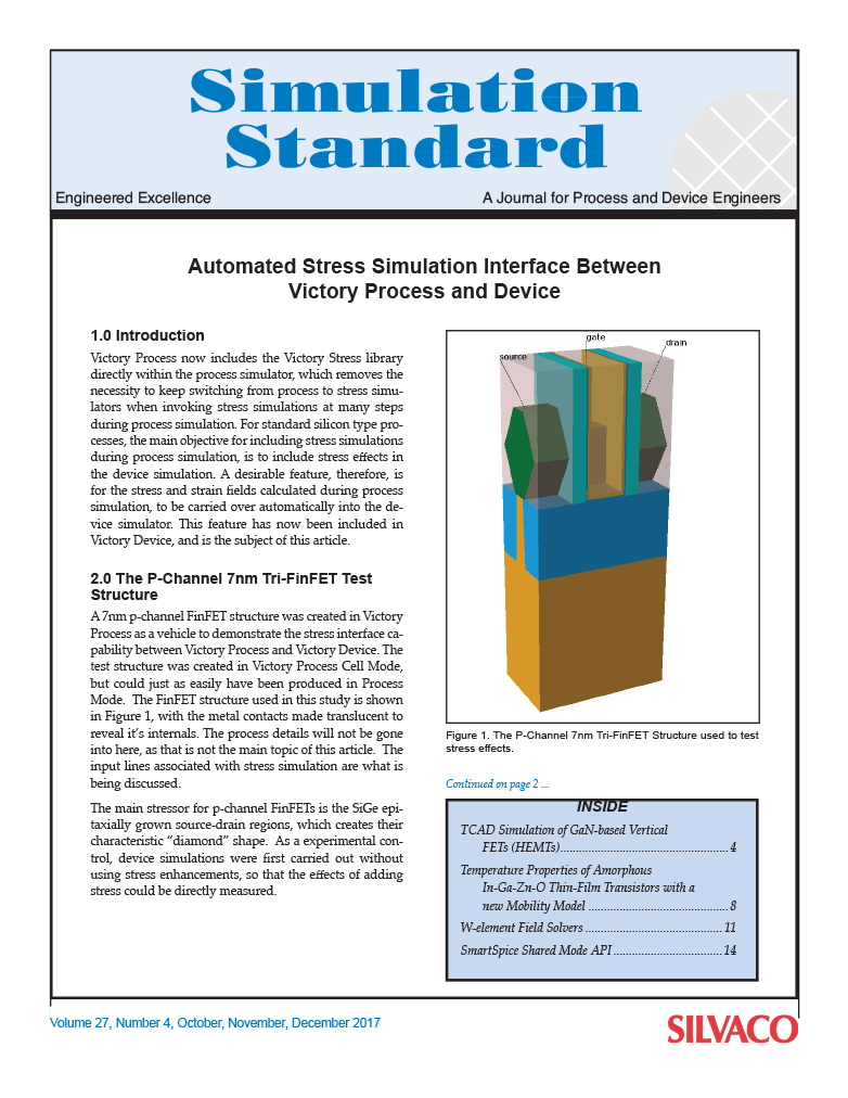
Automated Stress Simulation Interface Between Victory Process and Device
Victory Process now includes the Victory Stress library directly within the process simulator, which removes the necessity to keep switching from process to stress simulators when invoking stress simulations at many steps during process simulation. For standard silicon type processes, the main objective for including stress simulations during process simulation, is to include stress effects in the device simulation. A desirable feature, therefore, is for the stress and strain fields calculated during process simulation, to be carried over automatically into the device simulator. This feature has now been included in Victory Device, and is the subject of this article.
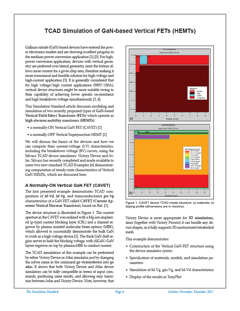
TCAD Simulation of GaN-based Vertical FETs (HEMTs)
Gallium nitride (GaN)-based devices have entered the power electronics market and are showing excellent progress in the medium power conversion application [1]-[5]. For high-power conversion application, devices with vertical geometry are preferred over lateral geometry, since the former allows more current for a given chip area, therefore making it more economical and feasible solution for high-voltage and high-current application [3]. It is generally considered that for high voltage/high current applications (900V/100A), vertical device structures might be more suitable owing to their capability of achieving lower specific on-resistance and high breakdown voltage simultaneously [3, 4].
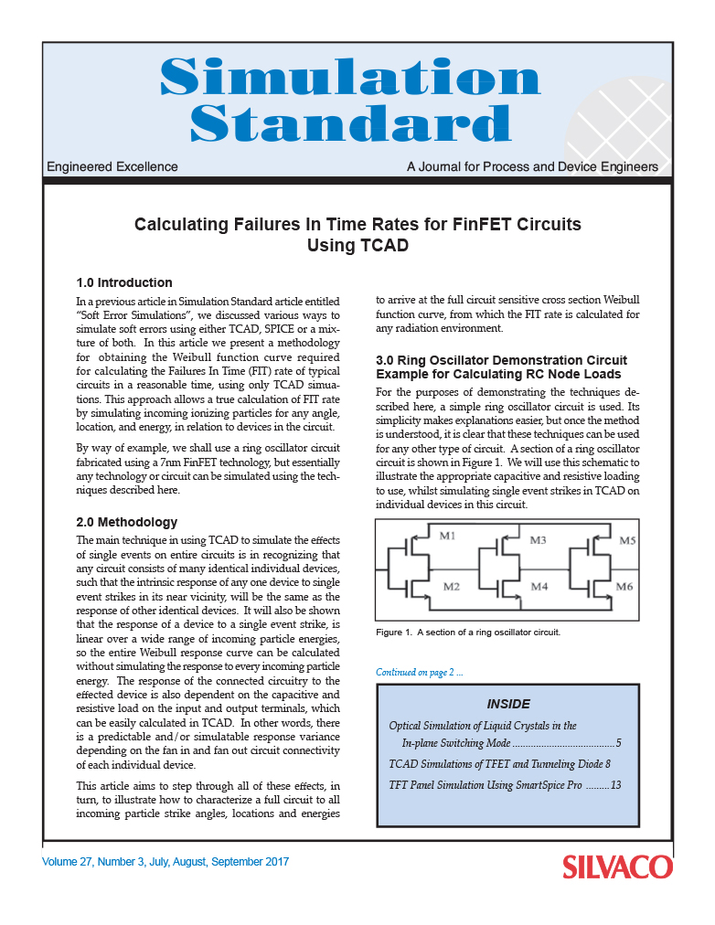
Calculating Failures In Time Rates for FinFET Circuits Using TCAD
In a previous article in Simulation Standard article entitled “Soft Error Simulations”, we discussed various ways to simulate soft errors using either TCAD, SPICE or a mixture of both. In this article we present a methodology for obtaining the Weibull function curve required for calculating the Failures In Time (FIT) rate of typical circuits in a reasonable time, using only TCAD simuations. This approach allows a true calculation of FIT rate by simulating incoming ionizing particles for any angle, location, and energy, in relation to devices in the circuit.
Optical Simulation of Liquid Crystals in the In-plane Switching Mode
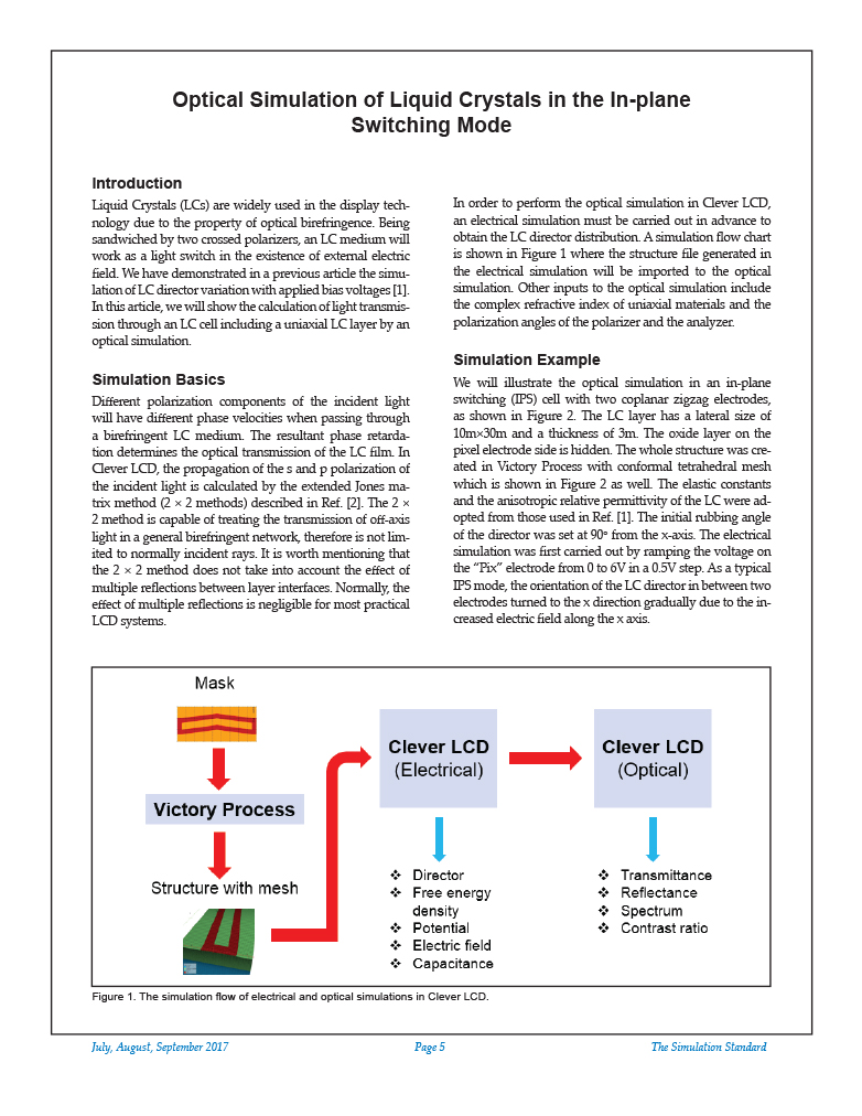
Liquid Crystals (LCs) are widely used in the display technology due to the property of optical birefringence. Being sandwiched by two crossed polarizers, an LC medium will work as a light switch in the existence of external electric field. We have demonstrated in a previous article the simulation of LC director variation with applied bias voltages [1]. In this article, we will show the calculation of light transmission through an LC cell including a uniaxial LC layer by an optical simulation.
TCAD Simulations of TFET and Tunneling Diode
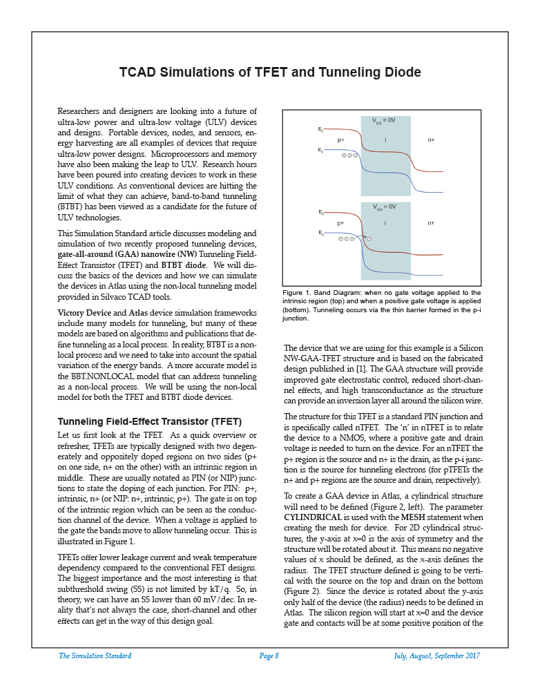
Researchers and designers are looking into a future of ultra-low power and ultra-low voltage (ULV) devices and designs. Portable devices, nodes, and sensors, energy harvesting are all examples of devices that require ultra-low power designs. Microprocessors and memory have also been making the leap to ULV. Research hours have been poured into creating devices to work in these ULV conditions. As conventional devices are hitting the limit of what they can achieve, band-to-band tunneling (BTBT) has been viewed as a candidate for the future of ULV technologies.

