
Simulation Standard
Silvaco面向半导体工艺和器件仿真工程师推出的技术刊物
 https://silvaco.com/wp-content/uploads/2019/04/VP_fig5.jpg
471
550
Erick Castellon
/wp-content/uploads/2019/11/silvaco-logo.png
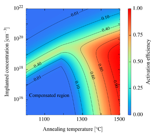
Erick Castellon2019-04-01 10:00:342021-10-13 09:39:13Process Simulation – New Features in 2019 Baseline Release
https://silvaco.com/wp-content/uploads/2019/04/VP_fig5.jpg
471
550
Erick Castellon
/wp-content/uploads/2019/11/silvaco-logo.png
Erick Castellon2019-04-01 10:00:342021-10-13 09:39:13Process Simulation – New Features in 2019 Baseline Release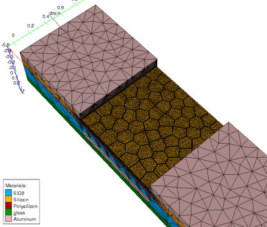 https://silvaco.com/wp-content/uploads/2020/03/fig11.jpg
469
550
Erick Castellon
/wp-content/uploads/2019/11/silvaco-logo.png
Erick Castellon2019-04-01 09:00:112021-10-13 09:39:13Meshing – New Features in 2019 Baseline Release
https://silvaco.com/wp-content/uploads/2020/03/fig11.jpg
469
550
Erick Castellon
/wp-content/uploads/2019/11/silvaco-logo.png
Erick Castellon2019-04-01 09:00:112021-10-13 09:39:13Meshing – New Features in 2019 Baseline Release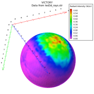 https://silvaco.com/wp-content/uploads/2019/04/device_fig2-6b.jpg
312
312
Erick Castellon
/wp-content/uploads/2019/11/silvaco-logo.png
Erick Castellon2019-04-01 08:00:192021-10-13 09:41:31Device Simulation – New Features in 2019 Baseline Release
https://silvaco.com/wp-content/uploads/2019/04/device_fig2-6b.jpg
312
312
Erick Castellon
/wp-content/uploads/2019/11/silvaco-logo.png
Erick Castellon2019-04-01 08:00:192021-10-13 09:41:31Device Simulation – New Features in 2019 Baseline Release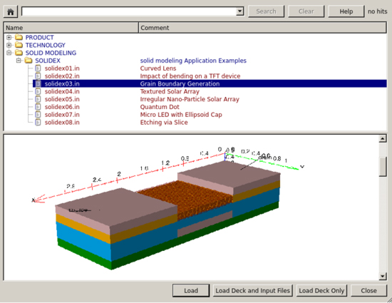 https://silvaco.com/wp-content/uploads/2020/03/DB_fig4-6.jpg
425
550
Erick Castellon
/wp-content/uploads/2019/11/silvaco-logo.png
Erick Castellon2019-04-01 07:00:592021-10-13 09:41:31Interactive Tools – New Features in 2019 Baseline Release
https://silvaco.com/wp-content/uploads/2020/03/DB_fig4-6.jpg
425
550
Erick Castellon
/wp-content/uploads/2019/11/silvaco-logo.png
Erick Castellon2019-04-01 07:00:592021-10-13 09:41:31Interactive Tools – New Features in 2019 Baseline Release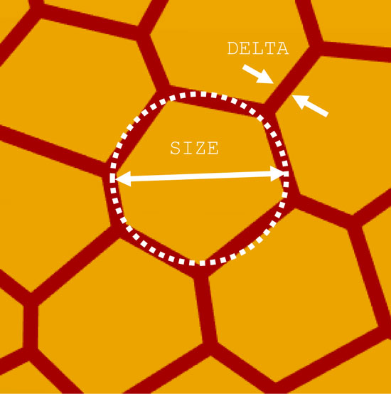 https://silvaco.com/wp-content/uploads/2020/03/3D_TFT_fig1.jpg
554
550
Erick Castellon
/wp-content/uploads/2019/11/silvaco-logo.png
Erick Castellon2019-01-01 10:00:392021-10-13 09:41:483D TFT Simulation of Grains and Grain Boundaries
https://silvaco.com/wp-content/uploads/2020/03/3D_TFT_fig1.jpg
554
550
Erick Castellon
/wp-content/uploads/2019/11/silvaco-logo.png
Erick Castellon2019-01-01 10:00:392021-10-13 09:41:483D TFT Simulation of Grains and Grain Boundaries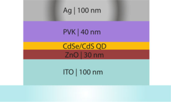 https://silvaco.com/wp-content/uploads/2020/03/hyLED__fig1a.jpg
329
550
Erick Castellon
/wp-content/uploads/2019/11/silvaco-logo.png
Erick Castellon2019-01-01 08:00:442021-10-13 09:41:54Quantum Dot-Based Hybrid Light Emitting Diode Modelling Using Radiant
https://silvaco.com/wp-content/uploads/2020/03/hyLED__fig1a.jpg
329
550
Erick Castellon
/wp-content/uploads/2019/11/silvaco-logo.png
Erick Castellon2019-01-01 08:00:442021-10-13 09:41:54Quantum Dot-Based Hybrid Light Emitting Diode Modelling Using Radiant